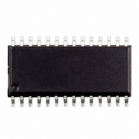
VN772KTR-E STMicroelectronics, VN772KTR-E Datasheet

VN772KTR-E
Specifications of VN772KTR-E
Available stocks
Related parts for VN772KTR-E
VN772KTR-E Summary of contents
Page 1
... MOSFET in VIPower™ technology). They have built-in thermal shutdown, linear current limitation and overvoltage clamping. Fault feedback for thermal monitoring the voltage at the input pin. Tube VN772K-E VN772K-E SO-28 to protect the chips intervention can be detected Tape and Reel VN772KTR-E Rev. 1 from by 1/21 ...
Page 2
VN772K-E Figure 2. Block Diagram V cc CLAMP GND INPUT1 DIAG LOGIC OVERTEMP. 1 INPUT2 OVERTEMP. 2 INPUT3 INPUT4 2/ OVERVOLTAGE UNDERVOLTAGE CLAMP 1 DRIVER 1 CURRENT LIMITER 1 OPENLOAD ON 1 OPENLOAD OFF 1 Overvoltage Gate Control ...
Page 3
Table 3. Pin Function No NAME 1, 3, 25, 28 DRAIN 3 2 INPUT N.C. 5, 10, 19 GND 7 INPUT 1 8 DIAGNOSTIC 9 INPUT 2 12, 14, 15, 18 DRAIN 4 ...
Page 4
VN772K-E ABSOLUTE MAXIMUM RATINGS Table 5. Dual High Side Switch Symbol V DC Supply Voltage Reverse DC Supply Voltage Reverse Ground Pin Current GND I DC Output Current OUT - I Reverse DC ...
Page 5
ELECTRICAL CHARACTERISTICS FOR DUAL HIGH SIDE SWITCH (8V<V <36V; -40°C< T <150°C, unless otherwise specified) (Per each channel Table 7. Power Outputs Symbol Parameter Operating Supply Voltage Undervoltage Shut-down ...
Page 6
VN772K-E ELECTRICAL CHARACTERISTICS FOR DUAL HIGH SIDE SWITCH (continued) Table 11. Protections Symbol Parameter T Shut-down Temperature TSD T Reset Temperature R T Thermal Hysteresis hyst Status Delay in Overload t SDL Conditions I Current limitation lim Turn-off Output Clamp ...
Page 7
ELECTRICAL CHARACTERISTICS FOR LOW SIDE SWITCHES (continued) (T =25°C, unless otherwise specified) j Table 15. Dynamic Symbol Parameter Forward g (*) fs Transconductance C Output Capacitance OSS Table 16. Switching Symbol Parameter t Turn-on Delay Time d(on) t Rise Time ...
Page 8
VN772K-E DUAL HIGH-SIDE SWITCH Figure 4. Switching Time Waveforms V OUTn dV /dt OUT (on) V INn t d(on) Table 19. Truth Table CONDITIONS Normal Operation Current Limitation Overtemperature Undervoltage Overvoltage Output Voltage > Output Current < I ...
Page 9
Figure 6. Typical Application Diagram VN772K-E 9/21 ...
Page 10
VN772K-E Figure 7. Waveforms INPUT n OUTPUT VOLTAGE STATUS INPUT n OUTPUT VOLTAGE STATUS INPUT n OUTPUT VOLTAGE STATUS n INPUT n OUTPUT VOLTAGE STATUS n INPUT n OUTPUT VOLTAGE STATUS ...
Page 11
Electrical Characterization For Dual High Side Switch Figure 8. Off State Output Current IL(off1) (uA) 2.5 2.25 Off state 2 Vcc=36V Vin=Vout=0V 1.75 1.5 1.25 1 0.75 0.5 0.25 0 -50 - (°C) Figure 9. ...
Page 12
VN772K-E Electrical Characterization For Dual High Side Switch (continued) Figure 14. Overvoltage Shutdown Vov ( -50 - (°C) Figure 15. Turn-on Voltage Slope dVout/dt(on) ...
Page 13
Electrical Characterization For Dual High Side Switch (continued) Figure 20. Status Leakage Current Ilstat (uA) 0.05 0.04 Vstat=5V 0.03 0.02 0.01 0 -50 - (°C) Figure 21. Openload On State Detection Threshold Iol (mA) 150 ...
Page 14
VN772K-E Electrical Characterization For Low Side Switches Figure 25. Static Drain Source On Resistance Rds(on) (mOhm) 500 Tj= - 40ºC 450 400 350 300 250 200 150 100 0.25 0.5 0.75 Id(A) Figure 26. Transconductance Gfs (S) ...
Page 15
Electrical Characterization For Low Side Switches (continued) Figure 31. Input Voltage Vs. Input Charge Vin( Vds=12V Id=3. Qg(nC) Figure 32. Switching Time Resistive Load t(us) 5.5 5 ...
Page 16
VN772K-E Electrical Characterization For Low Side Switches (continued) Figure 37. Source-Drain Diode Forward Characteristics Vsd (mV) 1000 950 Vin=0V 900 850 800 750 700 650 600 550 500 Id(A) Figure 38. Static Drain-Source On resistance ...
Page 17
Electrical Characterization For Low Side Switches (continued) Figure 43. Turn off drain source voltage slope dv/dt(v/us) 300 250 200 150 100 50 0 200 400 600 100 300 500 700 Rg(ohm) Figure 44. Current Limit Vs. Junction Temperature Ilim (A) ...
Page 18
VN772K-E Table 20. SO-28 Mechanical Data Symbol Figure 46. SO-28 Package Dimensions 18/21 millimeters Min Typ 0.10 0.35 0.23 0.50 45° (typ.) 17.7 10.00 1.27 16.51 7.40 ...
Page 19
Figure 47. SO-28 Tube Shipment (No Suffix Figure 48. Tape And Reel Shipment (Suffix “TR”) TAPE DIMENSIONS According to Electronic Industries Association (EIA) Standard 481 rev. A, Feb. 1986 Tape width Tape Hole Spacing P0 (± 0.1) Component ...
Page 20
VN772K-E REVISION HISTORY Date Revision Sep. 2004 1 - First Issue. 20/21 Description of Changes ...
Page 21
... No license is granted by implication or otherwise under any patent or patent rights of STMicroelectronics. Specifications mentioned in this publication are subject to change without notice. This publication supersedes and replaces all information previously supplied. STMicroelectronics products are not authorized for use as critical components in life support devices or systems without express written approval of STMicroelectronics ...


