VN31-11-E STMicroelectronics, VN31-11-E Datasheet - Page 4
VN31-11-E
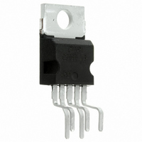
Manufacturer Part Number
VN31-11-E
Description
IC SMART PWR SSR ISO PENTAWATT-5
Manufacturer
STMicroelectronics
Type
High Sider
Datasheet
1.VN31-11-E.pdf
(13 pages)
Specifications of VN31-11-E
Input Type
Non-Inverting
Number Of Outputs
1
On-state Resistance
30 mOhm
Current - Output / Channel
11.5A
Current - Peak Output
31A
Voltage - Supply
5.5 V ~ 26 V
Operating Temperature
-40°C ~ 125°C
Mounting Type
Through Hole
Package / Case
Pentawatt-5 (Horizontal, Bent and Staggered Leads)
Mounting Style
Through Hole
Lead Free Status / RoHS Status
Lead free / RoHS Compliant


VN31
ELECTRICAL CHARACTERISTICS
(V
Table 5. Power
Note: 3. In= Nominal current according to ISO definition for high side automotive switch The Nominal Current is the current at T
Table 6. Switching
Note: 4. See Switching Time Waveforms.
Table 7. Logic Input
Note: 5. The V
4/13
V
Symbol
Symbol
(di/dt)
(di/dt)
Symbol
t
t
V
CC
DS(MAX)
d(on)
d(off)
V
V
I
demag
R
V
t
t
n
V
I(hyst)
r
V
f
I
I
CC
(4)
(4)
(3)
S
on
IN
ICL
IH
= 13 V; –40 ≤ T
IL
(4)
(4)
on
off
battery voltage of 13V which produces a voltage drop of 0.5 V.
to not exceed 10 mA at the input pin.
Supply Voltage
Nominal Current
On State Resistance
Supply Current
Maximum Voltage Drop
Turn-on Delay Time Of
Output Current
Rise Time Of Output
Current
Turn-off Delay Time Of
Output Current
Fall Time Of Output
Current
Turn-on Current Slope
Turn-off Current Slope
Inductive Load Clamp
Voltage
IH
Input Low Level Voltage
Input High Level Voltage
Input Hysteresis Voltage
Input Current
Input Clamp Voltage
is internally clamped at 6V about. It is possible to connect this pin to an higher voltage via an external resistor calculated
Parameter
Parameter
Parameter
j
≤ 125 °C unless otherwise specified)
T
I
I
I
I
Off State; T
On State
I
I
Input Rise Time < 0.1 µs
I
Input Rise Time < 0.1 µs
I
Input Rise Time < 0.1 µs
I
Input Rise Time < 0.1 µs
I
I
I
V
V
V
I
I
OUT
OUT
OUT
OUT
OUT
OUT
OUT
OUT
OUT
OUT
OUT
OUT
IN
IN
c
IN
IN
IN
= 85 °C; V
= 10 mA
= –10 mA
= 5 V
= 2 V
= 0.8 V
= 11.5 A
= 11.5 A; T
= 25 A; T
= 11.5 A; Resistive Load
= 11.5 A; Resistive Load
= 11.5 A; Resistive Load
= 11.5 A; Resistive Load
= 11.5 A
= I
= 11.5 A
= I
= 11.5 A; L = 1 mH
OV
OV
j
Test Conditions
≥ 25 °C
Test Conditions
Test Conditions
DS(on)
c
= 85 °C
j
= 25 °C
≤ 0.5
Min.
11.5
Min.
–24
Min.
5.5
5.5
25
2
Typ.
Typ.
0.08
Typ.
–0.7
100
140
–18
250
0.2
0.5
13
90
50
6
Note 5
Max.
–0.3
Max.
0.06
0.03
Max.
500
250
–14
0.8
1.5
0.5
26
50
15
1
3
3
c
= 85 °C for
Unit
Unit
A/µs
A/µs
A/µs
A/µs
Unit
mA
µA
µA
µA
µA
µs
µs
µs
µs
Ω
Ω
V
V
V
A
V
V
V
V
V
Related parts for VN31-11-E
Image
Part Number
Description
Manufacturer
Datasheet
Request
R

Part Number:
Description:
IC SSR HIGHSIDE PENTAWATT5 VERT
Manufacturer:
STMicroelectronics
Datasheet:
Part Number:
Description:
IC SSR HIGHSIDE PENTAWATT5 HORZ
Manufacturer:
STMicroelectronics
Datasheet:

Part Number:
Description:
IC SMART PWR SSR ISO PENTAWATT-5
Manufacturer:
STMicroelectronics
Datasheet:
Part Number:
Description:
IC SMART PWR SSR ISO PENTAWATT-5
Manufacturer:
STMicroelectronics
Datasheet:
Part Number:
Description:
IC SMART PWR SSR ISO PENTAWATT-5
Manufacturer:
STMicroelectronics
Datasheet:
Part Number:
Description:
STMicroelectronics [RIPPLE-CARRY BINARY COUNTER/DIVIDERS]
Manufacturer:
STMicroelectronics
Datasheet:
Part Number:
Description:
STMicroelectronics [LIQUID-CRYSTAL DISPLAY DRIVERS]
Manufacturer:
STMicroelectronics
Datasheet:

Part Number:
Description:
BOARD EVAL FOR MEMS SENSORS
Manufacturer:
STMicroelectronics
Datasheet:
Part Number:
Description:
NPN TRANSISTOR POWER MODULE
Manufacturer:
STMicroelectronics
Datasheet:
Part Number:
Description:
TURBOSWITCH ULTRA-FAST HIGH VOLTAGE DIODE
Manufacturer:
STMicroelectronics
Datasheet:
Part Number:
Description:
Manufacturer:
STMicroelectronics
Datasheet:
Part Number:
Description:
DIODE / SCR MODULE
Manufacturer:
STMicroelectronics
Datasheet: