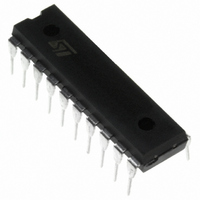
E-L6204 STMicroelectronics, E-L6204 Datasheet - Page 8

E-L6204
Manufacturer Part Number
E-L6204
Description
IC DRIVER FULL BRIDGE DUAL 20DIP
Manufacturer
STMicroelectronics
Type
H Bridger
Datasheet
1.E-L6204.pdf
(12 pages)
Specifications of E-L6204
Input Type
Non-Inverting
Number Of Outputs
4
On-state Resistance
1.2 Ohm
Current - Output / Channel
500mA
Current - Peak Output
3A
Voltage - Supply
12 V ~ 48 V
Operating Temperature
-40°C ~ 150°C
Mounting Type
Through Hole
Package / Case
20-DIP (0.300", 7.62mm)
Operating Supply Voltage
42 V
Supply Current
10 mA
Mounting Style
Through Hole
Current, Output, High Level
3 A
Package Type
20-Lead Power DIP, SO20
Power Dissipation
2 W
Temperature, Operating, Maximum
150 °C
Temperature, Operating, Minimum
-40 °C
Voltage, Input, High Level
7 V
Voltage, Input, Low Level
–0.3 V
Voltage, Supply
50 V
Lead Free Status / RoHS Status
Lead free / RoHS Compliant
Available stocks
Company
Part Number
Manufacturer
Quantity
Price
Part Number:
E-L6204
Manufacturer:
ST
Quantity:
20 000
L6204
APPLICATION INFORMATION
RECIRCULATION
During recirculation with the ENABLE input high, the voltage drop across the transistor is R
voltages less than 0.7 V and is clamped at a voltage depending on the characteristics of the source-drain
diode for greater voltages. Although the device is protected against cross conduction, current spikes can
appear on the current sense pin due to charge/discharge phenomena in the intrinsic source drain capac-
itances. In the application this does not cause any problems because the voltage created across the sense
resistor is usually much less than the peak value, although a small RC filter can be added if necessary.
POWER DISSIPATION (each bridge)
In order to achieve the high performance provided by the L6204 some attention must be paid to ensure
that it has an adequate PCB area to dissipate the heat. The first stage of any thermal design is to calculate
the dissipated power in the appl ication, for this example the half step operation shown in figure 7 is con-
sidered.
RISE TIME T
When an arm of the half bridge is turned on current begins to flow in the inductive load until the maximum
current I
The dissipated energy E
Figure 7.
ON TIME T
During this time the energy dissipated is due to the ON resistance of the transistors E
tation E
In the commutation the energy dissipated is :
Where :
T
T
f
8/12
SWITCH
COM
COM
= Commutation Time and it is assumed that ;
= T
COM
= Chopper frequency
L
TURN-ON
is reached after a time T
ON
. As two of the POWER DMOS transistors are ON E
r
= T
TURN-OFF
OFF/ON
= 100 ns
is in this case :
r
E
.
COM
E
OFF/ON
E
ON
= V
= I
S
= [R
· I
L
2
L
· R
DS(ON)
· T
DS(ON)
COM
· I
· f
L
SWITCH
· 2 · T
2
· T
r
] · 2/3
ON
ON
· T
is given by :
ON
ON
and the commu-
DS(ON)
. I
L
for


