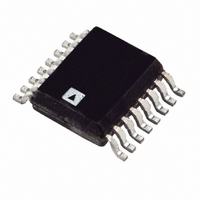
ADM869LARQ Analog Devices Inc, ADM869LARQ Datasheet - Page 3

ADM869LARQ
Manufacturer Part Number
ADM869LARQ
Description
IC SW HIGH-SIDE P-CH 16QSOP
Manufacturer
Analog Devices Inc
Type
High Sider
Datasheet
1.ADM869LARQ.pdf
(8 pages)
Specifications of ADM869LARQ
Number Of Outputs
6
Rohs Status
RoHS non-compliant
Input Type
Non-Inverting
On-state Resistance
45 mOhm
Current - Output / Channel
2A
Current - Peak Output
3A
Voltage - Supply
2.7 V ~ 5.5 V
Operating Temperature
-40°C ~ 85°C
Mounting Type
Surface Mount
Package / Case
16-QSOP
Input Voltage Range
2.7 to 5.5V
Number Of Inputs
1
Mounting
Surface Mount
Operating Temperature (max)
85C
Operating Temperature (min)
-40C
Operating Temperature Classification
Industrial
Lead Free Status / RoHS Status
Not Compliant
Available stocks
Company
Part Number
Manufacturer
Quantity
Price
Part Number:
ADM869LARQZ
Manufacturer:
ADI/亚德诺
Quantity:
20 000
ABSOLUTE MAXIMUM RATINGS*
(T
IN to GND . . . . . . . . . . . . . . . . . . . . . . . . . . . –0.3 V to +6 V
ON, FAULT to GND . . . . . . . . . . . . . . . . . . . –0.3 V to +6 V
SET, OUT to GND . . . . . . . . . . . . . . –0.3 V to (V
Maximum Continuous Switch Current . . . . . . . . . . . . . . . 3 A
Continuous Power Dissipation (T
Operating Temperature Range
Storage Temperature Range . . . . . . . . . . . . –65°C to +150°C
Lead Temperature (Soldering, 10 sec) . . . . . . . . . . . . . 300°C
ESD Rating (Outputs) . . . . . . . . . . . . . . . . . . . . . . . . . . 15 kV
*This is a stress rating only; functional operation of the device at these or any other
THERMAL CHARACTERISTICS
16-Lead QSOP Package:
θ
Model
ADM869LARQ –40°C to +85°C 16-Lead QSOP RQ-16
REV. B
Pin
1, 4, 5, 12, 13, 16
2, 3, 6, 11, 14, 15
7
8
9
10
CAUTION
ESD (electrostatic discharge) sensitive device. Electrostatic charges as high as 4000 V readily
accumulate on the human body and test equipment and can discharge without detection.
Although the ADM869L features proprietary ESD protection circuitry, permanent damage may
occur on devices subjected to high energy electrostatic discharges. Therefore, proper ESD
precautions are recommended to avoid performance degradation or loss of functionality.
conditions above those indicated in the operation sections of this specification is
not implied. Exposure to absolute maximum rating conditions for extended
periods of time may affect reliability.
JA
A
QSOP (Derate 8.3 mW/°C above 70°C)
Industrial (A Version) . . . . . . . . . . . . . . . . –40°C to +85°C
(Other Pins) . . . . . . . . . . . . . . . . . . . . . . . . . . . . . . . . . 2 kV
= 50°C/W, θ
= 25°C unless otherwise noted)
JC
= 10°C/W
Temperature
Range
ORDERING GUIDE
Mnemonic
OUT
ON
GND
SET
FAULT
IN
A
= 70°C) . . . . . . . 667 mW
Package
Description
Function
Input to P-Channel MOSFET Source and Supply to Chip Circuitry. Bypass IN with a 22 µF
capacitor to ground.
Output from P-Channel MOSFET Drain. Bypass OUT with a 0.1 µF capacitor to ground.
Digital Input. Active-low switch enable (logic 0 turns the switch on).
Ground.
Current Limit Setting Input. A resistor from set to ground sets the current limit. Refer to
Current Limit section.
Open-Drain Digital Output. FAULT goes low when the current limit is exceeded or the die
temperature exceeds 135°C. During startup, FAULT remains low for the turn-on time + 50 µs.
PIN FUNCTION DESCRIPTIONS
IN
Package
Option
+ 0.3 V)
–3–
OUT
GND
PIN CONFIGURATION
OUT
OUT
ON
IN
IN
IN
1
2
5
6
7
3
4
8
(Not to Scale)
ADM869L
TOP VIEW
16
15
14
13
12
11
10
9
OUT
OUT
IN
IN
IN
OUT
FAULT
SET
ADM869L


