IPS0151S International Rectifier, IPS0151S Datasheet - Page 2
IPS0151S
Manufacturer Part Number
IPS0151S
Description
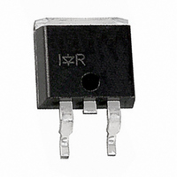
IC MOSFET PWR SWITCH D2PAK
Manufacturer
International Rectifier
Type
Low Sider
Datasheet
1.IPS0151.pdf
(13 pages)
Specifications of IPS0151S
Input Type
Non-Inverting
Number Of Outputs
1
On-state Resistance
20 mOhm
Current - Output / Channel
3.8A
Current - Peak Output
45A
Voltage - Supply
4 V ~ 6 V
Operating Temperature
-40°C ~ 150°C
Mounting Type
Surface Mount
Package / Case
D²Pak, TO-263 (2 leads + tab)
Lead Free Status / RoHS Status
Contains lead / RoHS non-compliant
Other names
*IPS0151S
Available stocks
Company
Part Number
Manufacturer
Quantity
Price
Company:

Part Number:
IPS0151S
Manufacturer:
IR
Quantity:
5 510
Company:
Part Number:
IPS0151S
Manufacturer:
XILINK
Quantity:
5 510


Recommended Operating Conditions
These values are given for a quick design. For operation outside these conditions, please consult the application notes.
IPS0151(S)
Thermal Characteristics
T r-in (max) Max recommended rise time for IN signal (see fig. 2)
(1) Limited by junction temperature (pulsed current limited also by internal wiring)
(2) Operations at higher switching frequencies is possible. See Application Notes.
Absolute Maximum Ratings
Absolute maximum ratings indicate sustained limits beyond which damage to the device may occur. All voltage parameters
are referenced to SOURCE lead. (T Ambient = 25
print with 70 m copper thickness.
Symbol Parameter
R th 1
R th 2
R th 1
R th 2
R th 3
Symbol Parameter
V ds (max) Continuous drain to source voltage
V IH
V IL
I ds
Tamb=85
R in
F r -I sc
Symbol Parameter
V ds
V in
I in, max
I sd
I sd
P d
ESD1
ESD2
T stor.
T j max.
T lead
2
cont.
pulsed
(2)
o
C
Thermal resistance free air
Thermal resistance junction to case
Thermal resistance with standard footprint
Thermal resistance with 1" square footprint
Thermal resistance junction to case
High level input voltage
Low level input voltage
Continuous drain current
Recommended resistor in series with IN pin
Max. frequency in short circuit condition (Vcc = 14V)
Maximum drain to source voltage
Maximum Input voltage
Maximum IN current
Diode max. continuous current
Diode max. pulsed current
Maximum power dissipation
Electrostatic discharge voltage
Electrostatic discharge voltage
Max. storage temperature
Max. junction temperature
Lead temperature (soldering, 10 seconds)
( TAmbient = 85
( TAmbient = 85
(rth=62
(rth=80
rth=62
rth=5
rth=80
o
C/W IPS015135
o
o
o
o
C/W) IPS0151
C/W) IPS0151S
C/W IPS0151
C/W IPS0151S
o
o
C, IN = 5V, rth = 60
C, IN = 5V, rth = 80
(1)
(1)
(Machine Model)
(Human Body)
(1)
o
C unless otherwise specified). PCB mounting uses the standard foot-
o
o
C/W, Tj = 125
C/W, Tj = 125
Min.
Min.
-0.3
-10
-55
-40
—
—
—
—
—
—
—
—
—
—
—
—
—
—
—
Typ.
Max.
+150
1.56
55
60
35
+10
300
150
2.8
2.2
0.5
47
35
45
2
2
7
2
4
o
o
C) IPS0151
C) IPS0151S
Max. Units Test Conditions
Units
—
a
—
—
—
mA
kV
o
V
A
W
C
o
C/W
TO220 free air
TO220 with Rth=5
SMD220 Std footprint
C=100pF, R=1500
C=200pF, R=0
TO-220
D
Min.
—
4
0
—
—
0.2
—
0
Test Conditions
2
PAK (SMD220)
Max.
0.5
4.3
3.8
35
5
1
1
6
L=10 H
o
C/W
www.irf.com
Units
kHz
k
A
S
V
Related parts for IPS0151S
Image
Part Number
Description
Manufacturer
Datasheet
Request
R

Part Number:
Description:
SCHOTTKY RECTIFIER
Manufacturer:
International Rectifier Corp.
Datasheet:
Part Number:
Description:
SCHOTTKY RECTIFIER
Manufacturer:
International Rectifier Corp.
Datasheet:
Part Number:
Description:
SCHOTTKY RECTIFIER
Manufacturer:
International Rectifier Corp.
Datasheet:
Part Number:
Description:
SCHOTTKY RECTIFIER
Manufacturer:
International Rectifier Corp.
Datasheet:
Part Number:
Description:
SCHOTTKY RECTIFIER
Manufacturer:
International Rectifier Corp.
Datasheet:
Part Number:
Description:
SCHOTTKY RECTIFIER
Manufacturer:
International Rectifier Corp.
Datasheet:
Part Number:
Description:
SCHOTTKY RECTIFIER
Manufacturer:
International Rectifier Corp.
Datasheet:
Part Number:
Description:
SCHOTTKY RECTIFIER
Manufacturer:
International Rectifier Corp.
Datasheet:
Part Number:
Description:
SCHOTTKY RECTIFIER
Manufacturer:
International Rectifier Corp.
Datasheet:
Part Number:
Description:
SCHOTTKY RECTIFIER
Manufacturer:
International Rectifier Corp.
Datasheet:
Part Number:
Description:
SCHOTTKY RECTIFIER
Manufacturer:
International Rectifier Corp.
Datasheet:
Part Number:
Description:
SCHOTTKY RECTIFIER
Manufacturer:
International Rectifier Corp.
Datasheet:
Part Number:
Description:
SCHOTTKY RECTIFIER
Manufacturer:
International Rectifier Corp.
Datasheet:
Part Number:
Description:
SCHOTTKY RECTIFIER
Manufacturer:
International Rectifier Corp.
Datasheet:
Part Number:
Description:
SCHOTTKY RECTIFIER
Manufacturer:
International Rectifier Corp.
Datasheet: