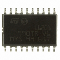
L6201 STMicroelectronics, L6201 Datasheet - Page 10

L6201
Manufacturer Part Number
L6201
Description
IC DRIVER FULL BRIDGE 20-SOIC
Manufacturer
STMicroelectronics
Type
H Bridger
Datasheet
1.L6201013TR.pdf
(20 pages)
Specifications of L6201
Input Type
Non-Inverting
Number Of Outputs
2
On-state Resistance
300 mOhm
Current - Output / Channel
1A
Current - Peak Output
2A
Voltage - Supply
12 V ~ 48 V
Operating Temperature
-40°C ~ 150°C
Mounting Type
Surface Mount
Package / Case
20-SOIC (7.5mm Width)
Operating Supply Voltage
12 V to 48 V
Supply Current
0.015 A
Mounting Style
SMD/SMT
Lead Free Status / RoHS Status
Lead free / RoHS Compliant
Other names
497-1418-5
Available stocks
Company
Part Number
Manufacturer
Quantity
Price
Part Number:
L6201
Manufacturer:
ST
Quantity:
20 000
Part Number:
L6201D013TR
Manufacturer:
ST
Quantity:
20 000
Part Number:
L6201P
Manufacturer:
ST
Quantity:
20 000
Part Number:
L6201P013TR
Manufacturer:
ST
Quantity:
20 000
Company:
Part Number:
L6201PS
Manufacturer:
STMicroelectronics
Quantity:
135
L6201 - L6202 - L6203
CIRCUIT DESCRIPTION
The L6201/1PS/2/3 is a monolithic full bridge
switching motor driver realized in the new Mul-
tipower-BCD technology which allows the integra-
tion of multiple, isolated DMOS power transistors
plus mixed CMOS/bipolar control circuits. In this
way it has been possible to make all the control
inputs TTL, CMOS and C compatible and elimi-
nate the necessity of external MOS drive compo-
nents. The Logic Drive is shown in table 1.
Table 1
L = Low
(*) Numbers referred to INPUT1 or INPUT2 controlled output stages
Although the device guarantees the absence of
cross-conduction, the presence of the intrinsic di-
odes in the POWER DMOS structure causes the
generation of current spikes on the sensing termi-
nals. This is due to charge-discharge phenomena
in the capacitors C1 & C2 associated with the
drain source junctions (fig. 14). When the output
switches from high to low, a current spike is gen-
erated associated with the capacitor C1. On the
low-to-high transition a spike of the same polarity
is generated by C2, preceded by a spike of the
opposite polarity due to the charging of the input
capacity of the lower POWER DMOS transistor
(fig. 15).
Figure 14: Intrinsic Structures in the POWER
10/20
V
V
EN
EN
= H
= L
Inputs
DMOS Transistors
H = High
IN1
H
H
X
L
L
IN2
H
H
X
L
L
X = DON’t care
All transistors turned oFF
Sink 1, Sink 2
Sink 1, Source 2
Source 1, Sink 2
Source 1, Source 2
Output Mosfets (*)
Figure 15: Current Typical Spikes on the Sens-
TRANSISTOR OPERATION
ON State
When one of the POWER DMOS transistor is ON
it can be considered as a resistor R
throughout the recommended operating range. In
this condition the dissipated power is given by :
The low R
can provide high currents with low power dissipa-
tion.
OFF State
When one of the POWER DMOS transistor is
OFF the V
age and only the leakage current I
power dissipation during this period is given by :
The power dissipation is very low and is negligible
in comparison to that dissipated in the ON
STATE.
Transitions
As already seen above the transistors have an in-
trinsic diode between their source and drain that
can operate as a fast freewheeling diode in
switched mode applications. During recirculation
with the ENABLE input high, the voltage drop
across the transistor is R
reaches the diode forward voltage it is clamped.
When the ENABLE input is low, the POWER
MOS is OFF and the diode carries all of the recir-
culation current. The power dissipated in the tran-
sitional times in the cycle depends upon the volt-
age-current waveforms and in the driving mode.
(see Fig. 7ab and Fig. 8abc).
DS (ON)
DS
P
ing Pin
ON
P
voltage is equal to the supply volt-
trans.
= R
P
of the Multipower-BCD process
OFF
DS (ON)
= I
= V
DS
(t) V
S
DS (ON)
I
DS
I
DSS
2
DS
(RMS)
(t)
I
DSS
D
and when it
flows. The
DS (ON)


