VN31 STMicroelectronics, VN31 Datasheet - Page 6
VN31
Manufacturer Part Number
VN31
Description
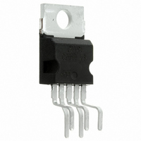
IC SSR HIGHSIDE PENTAWATT5 VERT
Manufacturer
STMicroelectronics
Type
High Sider
Datasheet
1.VN31-11-E.pdf
(13 pages)
Specifications of VN31
Input Type
Non-Inverting
Number Of Outputs
1
On-state Resistance
30 mOhm
Current - Output / Channel
11.5A
Current - Peak Output
31A
Voltage - Supply
5.5 V ~ 26 V
Operating Temperature
-40°C ~ 125°C
Mounting Type
Through Hole
Package / Case
Pentawatt-5 (Vertical, Bent and Staggered Leads)
Lead Free Status / RoHS Status
Lead free / RoHS Compliant
Available stocks
Company
Part Number
Manufacturer
Quantity
Price

Company:
Part Number:
VN319124
Manufacturer:
VISHAY
Quantity:
270
Part Number:
VN31SP
Manufacturer:
ST
Quantity:
20 000


VN31
Figure 7. Switching Time Waveforms
FUNCTIONAL DESCRIPTION
The device has a diagnostic output which
indicates open load conditions in off state as well
as in on state, output shorted to V
overtemperature. The truth table shows input,
diagnostic and output voltage level in normal
operation and in fault conditions. The output
signals are processed by internal logic. The open
load diagnostic output has a 5 ms filtering. The
filter gives a continuous signal for the fault
condition after an initial delay of about 5 ms. This
means that a disconnection during normal
operation, with a duration of less than 5 ms does
not affect the status output. Equally, any re-
connection
disconnection duration does not affect the status
output. No delay occur for the status to go low in
case of overtemperature conditions. From the
falling edge of the input signal the status output
initially low in fault condition (over temperature or
open load) will go back with a delay (t
of overtemperature condition and a delay (t
case of open load. These feature fully comply with
International Standard Office (I.S.O.) requirement
for automotive High Side Driver.
To protect the device against short circuit and over
current conditions, the thermal protection turns the
integrated Power MOS off at a minimum junction
temperature of 140 °C. When the temperature
returns to 125 °C the switch is automatically turned
on again. In short circuit the protection reacts with
virtually no delay, the sensor being located in the
region of the die where the heat is generated.
Driving inductive loads, an internal function of the
6/13
of
less
than
5
ms
povl
during
CC
)in case
pol
and
) in
a
device ensures the fast demagnetization with a
typical voltage (V
This function allows to greatly reduce the power
dissipation according to the formula:
P
V
where f = switching frequency and
V
Based on this formula it is possible to know the
value of inductance and/or current to avoid a
thermal shut-down. The maximum inductance
which causes the chip temperature to reach the
shut down temperature in a specific thermal
environment, is infact a function of the load current
for a fixed V
PROTECTING THE DEVICE AGAIST LOAD
DUMP - TEST PULSE 5
The device is able to withstand the test pulse No.
5 at level II (V
7637/1 without any external component. This
means that all functions of the device are
performed
disturbance at level II. The VN31 is able to
withstand the test pulse No.5 at level III adding an
external resistor of 150 ohm between pin 1 and
ground plus a filter capacitor of 1000 µF between
pin 3 and ground (if R
PROTECTING THE DEVICE AGAINST
REVERSE BATTERY
The simplest way to protect the device against a
continuous reverse battery voltage (-26V) is to
insert a Schottky diode between pin 1(GND) and
ground, as shown in the typical application circuit
(Figure 10).
The consequences of the voltage drop across this
diode are as follows:
– If the input is pulled to power GND, a negative
– The undervoltage shutdown level is increased
If there is no need for the control unit to handle
external analog signals referred to the power
GND, the best approach is to connect the
reference potential of the control unit to node [1]
(see application circuit in Figure 11), which
becomes the common signal GND for the whole
control board avoiding shift of V
This solution allows the use of a standard diode.
dem
demag
demag
voltage of -V
thresholds and V
respect to power GND).
by V
= 0.5 • L
f
] • f
.
= demagnetization voltage
CC
as
s
, V
= 46.5V) according to the ISO T/R
f
is seen by the device. (V
demag
load
demag
designed
STAT
LOAD
• (I
) of -18V.
and f.
are increased by V
load
≤ 20 Ω).
)
after
2
IH
• [(V
, V
exposure
IL
CC
and V
+V
demag
IL
f
STAT
, V
with
to
IH
)/
.
Related parts for VN31
Image
Part Number
Description
Manufacturer
Datasheet
Request
R

Part Number:
Description:
IC SSR HIGHSIDE PENTAWATT5 HORZ
Manufacturer:
STMicroelectronics
Datasheet:
Part Number:
Description:
IC SMART PWR SSR ISO PENTAWATT-5
Manufacturer:
STMicroelectronics
Datasheet:

Part Number:
Description:
IC SMART PWR SSR ISO PENTAWATT-5
Manufacturer:
STMicroelectronics
Datasheet:
Part Number:
Description:
IC SMART PWR SSR ISO PENTAWATT-5
Manufacturer:
STMicroelectronics
Datasheet:
Part Number:
Description:
IC SMART PWR SSR ISO PENTAWATT-5
Manufacturer:
STMicroelectronics
Datasheet:
Part Number:
Description:
STMicroelectronics [RIPPLE-CARRY BINARY COUNTER/DIVIDERS]
Manufacturer:
STMicroelectronics
Datasheet:
Part Number:
Description:
STMicroelectronics [LIQUID-CRYSTAL DISPLAY DRIVERS]
Manufacturer:
STMicroelectronics
Datasheet:

Part Number:
Description:
BOARD EVAL FOR MEMS SENSORS
Manufacturer:
STMicroelectronics
Datasheet:
Part Number:
Description:
NPN TRANSISTOR POWER MODULE
Manufacturer:
STMicroelectronics
Datasheet:
Part Number:
Description:
TURBOSWITCH ULTRA-FAST HIGH VOLTAGE DIODE
Manufacturer:
STMicroelectronics
Datasheet:
Part Number:
Description:
Manufacturer:
STMicroelectronics
Datasheet:
Part Number:
Description:
DIODE / SCR MODULE
Manufacturer:
STMicroelectronics
Datasheet: