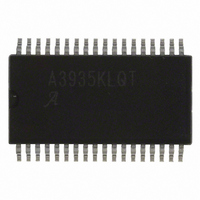
A3935KLQTR-T Allegro Microsystems Inc, A3935KLQTR-T Datasheet - Page 9

A3935KLQTR-T
Manufacturer Part Number
A3935KLQTR-T
Description
IC CTLR MOSFET 3PH AUTO 36-SOIC
Manufacturer
Allegro Microsystems Inc
Datasheet
1.A3935KLQTR-T.pdf
(12 pages)
Specifications of A3935KLQTR-T
Applications
DC Motor Driver, Brushless (BLDC), 3 Phase
Number Of Outputs
1
Voltage - Load
7 V ~ 40 V
Voltage - Supply
4.75 V ~ 5.25 V
Operating Temperature
-40°C ~ 135°C
Mounting Type
Surface Mount
Package / Case
36-QSOP
Device Type
Full Bridge
Peak Output Current
1.6mA
Output Resistance
8ohm
Input Delay
150ns
Output Delay
150ns
Supply Voltage Range
4.75V To 5.25V
Driver Case Style
QSOP
No. Of Pins
36
Lead Free Status / RoHS Status
Lead free / RoHS Compliant
Current - Output
-
Lead Free Status / RoHS Status
Lead free / RoHS Compliant, Lead free / RoHS Compliant
Other names
620-1292-2
A3935KLQTR-T
A3935KLQTR-T
Available stocks
Company
Part Number
Manufacturer
Quantity
Price
Part Number:
A3935KLQTR-T
Manufacturer:
ALLEGRO/雅丽高
Quantity:
20 000
A3935
Motor Lead Protection. A fault detection circuit monitors
the voltage across the drain-to-source of the external MOSFETs.
A fault is asserted low on the output terminal, ¯ F ¯ ¯ A ¯ ¯ U ¯ ¯ L ¯ ¯ T ¯ , if the
drain-to-source voltage of any MOSFET that is instructed to
turn on is greater than the voltage applied to the V
terminal. When a high-side switch is turned on, the voltage from
V
If the motor lead is shorted to ground before the high-side is
turned on, the measured voltage will exceed the threshold and
the ¯ F ¯ ¯ A ¯ ¯ U ¯ ¯ L ¯ ¯ T ¯ terminal will go low. Similarly, when a low-side
MOSFET is turned on, the differential voltage between the motor
phase (drain) and the LSS terminal (source) is monitored. V
is set by a resistor divider to V
The V
high-side, drain-to-source monitor circuit. Voltage drops across
the power bus are eliminated by connecting an isolated PCB trace
from the V
This allows improved accuracy in setting the V
voltage. The low-side, drain-to-source monitor uses the LSS
terminal, rather than V
The A3935 just reports these motor faults.
Fault Outputs. Transient faults on any of the fault outputs
are to be expected during switching, and will not disable the
gate drive outputs. External circuitry or controller logic must
determine if the faults represent a hazardous condition.
¯
ing conditions occur:
resets low after a recovery hysteresis. It has a high-impedance
state when a thermal shutdown or V
voltage at the OVSET terminal, V
voltage set point V
F ¯ ¯ A ¯ ¯ U ¯ ¯ L ¯ ¯ T ¯ . This terminal will go active low when any of the follow-
OVFLT. Asserts high when a V
• V
• V
• V
• Motor lead short-to-ground
DRAIN
BAT
BAT
REG
DRAIN
to the appropriate motor phase output, V
overvoltage
undervoltage
undervoltage
DRAIN
is intended to be a Kelvin connection for the
terminal to the drain of the MOSFET bridge.
BAT(ov)
DRAIN
, as follows:
, for comparison with V
DD
3-Phase Power MOSFET Controller for Automotive Applications
BAT
• Motor lead short-to-supply
• Bridge (or V
• V
• Thermal shut down
.
OVSET
or short-to-battery
DD
overvoltage fault occurs and
DD
undervoltage
undervoltage occurs. The
, controls the V
DRAIN
DSTH
SX
DSTH
Functional Description
, is examined.
DSTH
threshold
) open
BAT
input
.
over-
DSTH
V
formula to be valid, all variables must be in range and below the
maximum operating specification.
UVFLT. Asserts high when a V
resets low after exceeding a recovery hysteresis. It has a high-
impedance state when a thermal shut down or V
occurs. OVFLT and UVFLT are mutually exclusive by definition.
Current Sensing. A current-sense amplifier is provided to
allow system monitoring of the load current. The differential
amplifier inputs are intended to be Kelvin-connected across a
low-value sense resistor or current shunt. The output voltage is
represented by:
where V
and A
the CSP or CSN pin is open, the CSOUT pin will go to its
maximum positive level.
Shut Down. If a fault occurs because of excessive junction
temperature or undervoltage on V
outputs are driven low until the fault condition is removed. In
addition, the boost supply switch and VREG are turned off until
those undervoltages and junction temperatures recover.
Boost Supply. V
control loop, and by an outer voltage-feedback loop. The
current-control loop turns off the boost switch for 5 μs whenever
the voltage across the boost current-sense resistor exceeds
500 mV. A diode reverse-recovery current flows through the
sense resistor whenever the boost switch turns on, which could
result in turning off the switch again if not for the blanking-time
circuit. Adjustment of this external sense resistor determines the
maximum current in the inductor. Whenever V
predefined threshold, 16 V nominal the boost switch is inhibited.
where A
BAT(ov)
V
is the differential amplifier gain of about 19.2. If either
OS
BAT(ov)
V
V
when V
BAT(ov)
CSOUT
is the output voltage calibrated at zero load current
is the gain (12) and V
SET(ov)
= ( I
= (A
BOOST
LOAD
BAT(ov)
= 0 (V
is controlled by an inner current-
×A
115 Northeast Cutoff, Box 15036
Allegro MicroSystems, Inc.
Worcester, Massachusetts 01615-0036 (508) 853-5000
www.allegromicro.com
× V
V
BAT(ov)
BAT
× R
SET(ov)
DD
undervoltage fault occurs and
SENSE
or V
BAT(ov)(0)
≈ 22.4). For the above
) + V
) + V
BAT
BAT(ov)(0)
, all gate driver
OS
BOOST
is the value of
DD
undervoltage
,
exceeds the
9


