SA01 Cirrus Logic Inc, SA01 Datasheet - Page 4
SA01
Manufacturer Part Number
SA01
Description
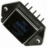
IC PWM AMP 100V 20A 10-PWRDIP
Manufacturer
Cirrus Logic Inc
Series
Apex Precision Power™r
Datasheet
1.SA01.pdf
(5 pages)
Specifications of SA01
Mfg Application Notes
SAxx App Note 34
Applications
DC Motor Controller, Brushless (BLDC)
Number Of Outputs
1
Current - Output
20A
Voltage - Supply
16 V ~ 100 V
Operating Temperature
-55°C ~ 125°C
Mounting Type
Through Hole
Package / Case
10-DIP Module
For Use With
598-1455 - EVALUATION KIT FOR SA01
Lead Free Status / RoHS Status
Lead free / RoHS Compliant
Voltage - Load
-
Other names
598-1362
Available stocks
Company
Part Number
Manufacturer
Quantity
Price

Part Number:
SA01
Manufacturer:
APEX
Quantity:
20 000
Company:
Part Number:
SA010M1000AZF-1015
Manufacturer:
YAGEO
Quantity:
260 000
Company:
Part Number:
SA010M1000AZF-1019
Manufacturer:
YAGEO
Quantity:
260 000
Company:
Part Number:
SA010M4700B7F-1625
Manufacturer:
YAGEO
Quantity:
260 000
Company:
Part Number:
SA016M0100AZF-0611
Manufacturer:
YAGEO
Quantity:
260 000


SA01 • SA01-6
4
GENERAL
to Application Note 1 "General Operating Considerations" for
helpful information regarding power supplies, heat sinking
and mounting. Visit www.Cirrus.com for design tools that help
automate pwm filter design; heat sink selection; Apex Precision
Power’s complete Application Notes library; Technical Seminar
Workbook; and Evaluation Kits.
CURRENT LIMIT
pin 8 (Isense). This limits load current and also limits current
in the event of a short of either output to +Vs. This circuit can
trip anytime during the conduction period and will hold the
output transistors off for the remainder of that conduction period.
be connected as shown in the external connection diagram.
It is recommended that the resistor be a non-inductive type.
Load current flows in pin 8. No current flows in pin 10 (Shut-
down/filter) so no error will be introduced by the length of
the connection to pin 10. However, the voltage at pin 10 is
compared to GND (pin 4) and an error could be introduced if
the grounded end of R
circuit board layout practice would be to connect R
between pins 8 and 4.
amplitude and duration will be load dependent. The noise
spikes could trip the current limit threshold which is only 200
mV. R
switching noise well below 200 mV to prevent false current
limiting. The sum of the DC level plus the noise peak will de-
termine the current limiting value. Suggested starting values
are C
maximum desired current.
SHUTDOWN
limiting circuitry. The two functions may be externally combined
as shown below in Figure 1. R
value resistor and can be considered zero for this application.
R
After a suitable noise filter is designed for the current limit
adjust the value of R
pin 10 when the shutdown signal is high. This means pin 10
will reach the 200 mV trip point in about one time constant
SHUTDOWN
FIGURE 1.
SD
Please read Application Note 30 on "PWM Basics". Refer
The current limit function sets a peak limit on current flow in
For proper operation the current limit sense resistor must
Switching noise spikes will invariably be found at pin 8. The
The required value of R
where R
The shutdown circuitry makes use of the internal current
SIGNAL
and R
FILTER
C
FILTER
FILTER
FILTER
= .01µF, R
and C
LIMIT
R
R
SD
LIMIT
form a voltage divider for the shutdown signal.
is the required resistor value, and I
FILTER
R
SHDN/FILTER
FILTER
SD
FILTER
should be adjusted so as to reduce the
R
LIMIT
to give 317 mV of shutdown signal at
I
SENSE
LIMIT
10
8
= 5k.
LIMIT
is not directly tied to pin 4. Good
= .2 V / I
may be calculated by:
LIMIT
will normally be a very low
with low output current and
less time as output current
increases. The voltage at
pin 10 is referenced to pin
4 (GND). C
both the current limit noise
spikes and the shutdown
signal. Shutdown and
current limit operate on
each cycle of the internal
switching rate. As long as
LIMIT
FILTER
LIMIT
LIMIT
will filter
directly
is the
P r o d u c t I n n o v a t i o n F r o m
the shutdown signal is high the output will be disabled.
PROTECTION CIRCUITS
sistors off. The first of these conditions is activation of the high
side current limit. Specifically, current in pin 7 (+V
tored. The DC trip level is about 35A and response time about
5us. As actual currents increase the response time decreases.
The external fault generally associated with this condition is
shorting one of the outputs to ground. However, a load fault
can also activate this high side current limit if the current rise
time is less than the response time of the filter discussed under
“Current Limit” . The second of these conditions is activation of
any of the four output transistor over-temperature sensors at
about 165°C. Ambient temperature, air flow, amplifier mounting
problems and all the previously mentioned high current faults
contribute to junction temperature. When either of these pro-
tection circuits are activated, the root fault must be corrected
and power cycled to restore normal operation.
DEAD TIME
put. The dead time removes the possibility of a momentary
conduction path through the upper and lower transistors of
each half bridge output during the switching interval. During
the dead time all output transistors are off. Noise or flyback
may be observed at the outputs during this time due to the
high impedance of the outputs in the off state. This will vary
with the nature of the load.
ERROR AMPLIFIER
highest loop accuracy it is best to configure the op amp as an
integrator (See Figure 2). Feedback can be adjusted with ap-
propriate poles and zeroes to properly compensate the velocity
loop for optimum stability.
ated internally. The non-inverting input of the op amp does not
have a common mode range which includes ground. R2 and
R7 are used with the reference voltage provided at pin 5 to
bias the non-inverting input to +5 volts, which is approximately
half of the voltage supplied internally to the op amp. Similarly,
R1 and the parallel combination of R5 R6 are selected to bias
the inverting input also at +5 volts. Resistors R1 R2 must be
matched. Likewise the parallel combination of R5 R6 must
be matched with R7. The source impedances of the tach
and the signal source may affect the matching and should be
considered in the design.
There are two conditions which will latch all the output tran-
There is a dead time between the on and off of each out-
The internal error amplifier is an operational amplifier. For
The op amp is operated from a single supply voltage gener-
TO TACH
SIGNAL
FIGURE 2.
C2
R5
R6
R4
REF OUT
R2
R7
+IN
–IN
5
1
2
R1
C1
.1µF
R3
E/A OUT
3
S
) is moni-
SA01U
Related parts for SA01
Image
Part Number
Description
Manufacturer
Datasheet
Request
R

Part Number:
Description:
Development Kit
Manufacturer:
Cirrus Logic Inc
Datasheet:
Part Number:
Description:
Development Kit
Manufacturer:
Cirrus Logic Inc
Datasheet:


Part Number:
Description:
High-efficiency PFC + Fluorescent Lamp Driver Reference Design
Manufacturer:
Cirrus Logic Inc
Datasheet:
Part Number:
Description:
Development Kit
Manufacturer:
Cirrus Logic Inc
Datasheet:
Part Number:
Description:
Development Kit
Manufacturer:
Cirrus Logic Inc
Datasheet:

Part Number:
Description:
Development Kit
Manufacturer:
Cirrus Logic Inc
Datasheet:
Part Number:
Description:
Development Kit
Manufacturer:
Cirrus Logic Inc
Datasheet:
Part Number:
Description:
Development Kit
Manufacturer:
Cirrus Logic Inc
Datasheet:
Part Number:
Description:
Development Kit
Manufacturer:
Cirrus Logic Inc
Datasheet:

Part Number:
Description:
EVALUATION BOARD FOR CS8427
Manufacturer:
Cirrus Logic Inc
Datasheet:

Part Number:
Description:
BOARD EVAL FOR CS8416 RCVR
Manufacturer:
Cirrus Logic Inc
Datasheet:

Part Number:
Description:
EVALUATION BOARD FOR CS8420
Manufacturer:
Cirrus Logic Inc
Datasheet:

Part Number:
Description:
KIT DEVELOPMENT EP9315 ARM9
Manufacturer:
Cirrus Logic Inc
Datasheet:

Part Number:
Description:
KIT DEVELOPMENT EP9302 ARM9
Manufacturer:
Cirrus Logic Inc
Datasheet: