SA08 Cirrus Logic Inc, SA08 Datasheet - Page 4
SA08
Manufacturer Part Number
SA08
Description
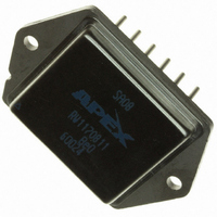
IC PWM AMP 450V 20A 12-PWRDIP
Manufacturer
Cirrus Logic Inc
Series
Apex Precision Power™r
Datasheet
1.SA08.pdf
(5 pages)
Specifications of SA08
Mfg Application Notes
SAxx App Note 34
Applications
PWM Motor Driver
Number Of Outputs
1
Current - Output
20A
Voltage - Load
16 V ~ 450 V
Voltage - Supply
14 V ~ 16 V
Operating Temperature
-55°C ~ 125°C
Mounting Type
Through Hole
Package / Case
12-DIP Module
For Use With
598-1460 - EVALUATION KIT FOR SA08
Lead Free Status / RoHS Status
Contains lead / RoHS compliant by exemption
Other names
598-1363
Available stocks
Company
Part Number
Manufacturer
Quantity
Price

Part Number:
SA08-21SRWA
Manufacturer:
KINGBRIGHT
Quantity:
20 000
Company:
Part Number:
SA0834
Manufacturer:
TDK-EPCOS
Quantity:
5 510


SA08
GENERAL
to Application Note 1 "General Operating Considerations" for
helpful information regarding power supplies, heat sinking
and mounting. Visit www.Cirrus.com for design tools that help
automate pwm filter design; heat sink selection; Apex Precision
Power’s complete Application Notes library; Technical Seminar
Workbook; and Evaluation Kits.
CLOCK CIRCUIT AND RAMP GENERATOR
proximately 45kHz. The CLK OUT pin will normally be tied to
the CLK IN pin. The clock is divided by two and applied to an
RC network which produces a ramp signal. An external clock
signal can be applied to the CLK IN pin for synchronization
purposes, but must be 45 kHz +/- 2%.
FLAG OUTPUT
output is set high (10V). When the programmable low side
current limit is exceeded, the FLAG output will be set high.
The FLAG output will be reset low on the next clock cycle. This
reflects the pulse-by-pulse current limiting feature. When the
internally-set high side current limit is tripped or the thermal
limit is reached, the FLAG output is latched high. See PRO-
TECTION CIRCUITS below.
PROTECTION CIRCUITS
Should either of the outputs be shorted to ground the high side
current limit will latch off the output transistors. The temperature
of the output transistors is also monitored. Should a fault condi-
tion raise the temperature of the output transistors to 165°C
the thermal protection circuit latch off the output transistors.
The latched condition can be cleared by either recycling the
V
a 10V pulse. See Figures A and B. The outputs will remain off
as long as the shutdown pulse is high (10V).
CURRENT LIMIT
SENSE B. The two pins can be shorted in the voltage mode
connection but both must be used in the current mode connec-
tion (see figures A and B). It is recommended that R
be non-inductive. Load current flows in the I SENSE pins. To
avoid errors due to lead lengths connect the I LIMIT/SHDN pin
directly to the R
shutdown divider resis-
tor) and connect the
R
to the GND pin.
spikes will invariably
be found at the I SENSE
pins. The noise spikes
could trip the current
limit threshold which
is only 100 mV. R
and C
4
CC
LIMIT
Please read Application Note 30 on "PWM Basics". Refer
The clock frequency is internally set to a frequency of ap-
Whenever the SA08 has detected a fault condition, the flag
Sw i t c h i n g n o i s e
There are two load current sensing pins, I SENSE A and I
A fixed internal current limit senses the high side current.
and +V
resistors directly
FILTER
S
should be
power or by toggling the I LIMIT/SHDN input with
LIMIT
FILTER
resistors (through the filter network and
I LIMIT/SHDN
FIGURE A. CURRENT LIMIT WITH
SHUTDOWN VOLTAGE MODE.
I SENSE A
I SENSE B
R
C
FILTER
FILTER
R
LIMIT
1N4148
5K
LIMIT
SHUTDOWN
resistors
SIGNAL
0/10V
P r o d u c t T e c h n o l o g y F r o m
grounding of the oscilloscope probe. Use the shortest possible
ground lead for the probe and connect exactly at the GND
terminal of the amplifier. Suggested starting values are C
= .1uF, R
culated by:
maximum desired current. In current mode the required value
of each R
divided down by 2 (see Figure B). If R
divide down the sense voltage. The shutdown divider network
will also have an effect on the filtering circuit.
BYPASSING
proper operation. Failure to do so can cause erratic and low
efficiency operation as well as excessive ringing at the out-
puts. The Vs supply should be bypassed with at least a 1µF
ceramic capacitor in parallel with another low ESR capacitor
of at least 10µF per amp of output current. Capacitor types
rated for switching applications are the only types that should
be considered. The bypass capacitors must be physically
connected directly to the power supply pins. Even one inch of
lead length will cause excessive ringing at the outputs. This
is due to the very fast switching times and the inductance of
the lead connection. The bypassing requirements of the Vcc
supply are less stringent, but still necessary. A .1µF to .47µF
ceramic capacitor connected directly to the Vcc pin will suffice.
STARTUP CONDITIONS
bootstrap circuit and charge pump arrangement. In order for
the circuit to produce a 100% duty cycle indefinitely the low
side of each half bridge circuit must have previously been in
the ON condition. This means, in turn, that if the input signal
to the SA08 at startup is demanding a 100% duty cycle, the
output may not follow the command and may be in a tri-state
condition. The ramp signal must cross the input signal at some
point to correctly determine the output state. After the ramp
crosses the input signal level one time, the output state will
be correct thereafter.
FIGURE B. CURRENT LIMIT WITH
SHUTDOWN CURRENT MODE.
I LIMIT/SHDN
I SENSE A
I SENSE B
The required value of R
where R
Adequate bypassing of the power supplies is required for
The high side of the IGBT output bridge circuit is driven by
R
LIMIT
FILTER
LIMIT
LIMIT
R
C
is 2 times this value since the sense voltage is
FILTER
= 5k .
is the required resistor value, and I
FILTER
R
5K
5K
LIMIT
R
LIMIT
LIMIT
1N4148
= .1 V / I
SHUTDOWN
in voltage mode may be cal-
SIGNAL
0/10V
LIMIT
SHDN
is used it will further
reduce the switch-
ing noise well below
100 mV to prevent
false current limit-
ing. The sum of the
DC level plus the
noise peak will de-
termine the current
limiting value. As
in most switching
circuits it may be
difficult to deter-
mine the true noise
amplitude without
careful attention to
adjusted so as to
LIMIT
SA08U
is the
FILTER
Related parts for SA08
Image
Part Number
Description
Manufacturer
Datasheet
Request
R

Part Number:
Description:
Development Kit
Manufacturer:
Cirrus Logic Inc
Datasheet:
Part Number:
Description:
Development Kit
Manufacturer:
Cirrus Logic Inc
Datasheet:


Part Number:
Description:
High-efficiency PFC + Fluorescent Lamp Driver Reference Design
Manufacturer:
Cirrus Logic Inc
Datasheet:
Part Number:
Description:
Development Kit
Manufacturer:
Cirrus Logic Inc
Datasheet:
Part Number:
Description:
Development Kit
Manufacturer:
Cirrus Logic Inc
Datasheet:

Part Number:
Description:
Development Kit
Manufacturer:
Cirrus Logic Inc
Datasheet:
Part Number:
Description:
Development Kit
Manufacturer:
Cirrus Logic Inc
Datasheet:
Part Number:
Description:
Development Kit
Manufacturer:
Cirrus Logic Inc
Datasheet:
Part Number:
Description:
Development Kit
Manufacturer:
Cirrus Logic Inc
Datasheet:

Part Number:
Description:
EVALUATION BOARD FOR CS8427
Manufacturer:
Cirrus Logic Inc
Datasheet:

Part Number:
Description:
BOARD EVAL FOR CS8416 RCVR
Manufacturer:
Cirrus Logic Inc
Datasheet:

Part Number:
Description:
EVALUATION BOARD FOR CS8420
Manufacturer:
Cirrus Logic Inc
Datasheet:

Part Number:
Description:
KIT DEVELOPMENT EP9315 ARM9
Manufacturer:
Cirrus Logic Inc
Datasheet:

Part Number:
Description:
KIT DEVELOPMENT EP9302 ARM9
Manufacturer:
Cirrus Logic Inc
Datasheet: