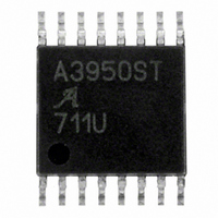
A3950SLP-T Allegro Microsystems Inc, A3950SLP-T Datasheet - Page 10

A3950SLP-T
Manufacturer Part Number
A3950SLP-T
Description
IC MOTOR DRIVER PWM FULL 16-TSSO
Manufacturer
Allegro Microsystems Inc
Datasheet
1.A3950SLP-T.pdf
(12 pages)
Specifications of A3950SLP-T
Applications
PWM Motor Driver
Number Of Outputs
1
Current - Output
±2.8A
Voltage - Supply
8 V ~ 36 V
Operating Temperature
-20°C ~ 85°C
Mounting Type
Surface Mount
Package / Case
16-TSSOP Exposed Pad, 16-eTSSOP, 16-HTSSOP
Operating Current
8.5mA
Operating Temperature Classification
Commercial
Package Type
TSSOP EP
Operating Supply Voltage (max)
36V
Lead Free Status / RoHS Status
Lead free / RoHS Compliant
Voltage - Load
-
Lead Free Status / RoHS Status
Compliant, Lead free / RoHS Compliant
Other names
620-1064
A3950
SENSE Pin. A low value resistor can be placed between the
SENSE pin and ground for current sensing purposes. To mini-
mize ground-trace IR drops in sensing the output current level,
the current sensing resistor should have an independent ground
return to the star ground point. This trace should be as short as
possible. For low value sense resistors, the IR drops in the PCB
can be significant, and should be taken into account.
When selecting a value for the sense resistor be sure not to
exceed the maximum voltage on the SENSE pin of ±500 mV.
Ground. A star ground should be located as close to the A3950
as possible. The copper ground plane directly under the exposed
thermal pad makes a good location for the star ground point. The
exposed pad can be connected to ground for this purpose.
GND
OUTA
U1
CVBB2
EU package shown
C1
C2
C3
OUTB
VBB
GND
CVBB1
DMOS Full-Bridge Motor Driver
Layout.
plane. For optimum electrical and thermal performance, the
A3950 must be soldered directly onto the board. On the under-
side of the A3950 package is an exposed pad, which provides a
path for enhanced thermal dissipation. The thermal pad should be
soldered directly to an exposed surface on the PCB. Thermal vias
are used to transfer heat to other layers of the PCB.
The load supply pin, VBB, should be decoupled with an elec-
trolytic capacitor (typically 100 μF) in parallel with a ceramic
capacitor placed as close as possible to the device. The ceramic
capacitors between VCP and VBB, connected to VREG, and
between CP1 and CP2, should be as close to the pins of the
device as possible, in order to minimize lead inductance.
The printed circuit board should use a heavy ground-
PHASE
GND
SLEEP
ENABLE
EU Package
A3950
PAD
115 Northeast Cutoff, Box 15036
Allegro MicroSystems, Inc.
Worcester, Massachusetts 01615-0036 (508) 853-5000
www.allegromicro.com
C1
OUTB
CVBB2
GND
CP2
CP1
C2
V
BB
C3
CVBB1
10


