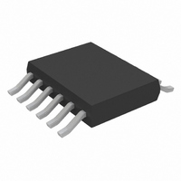
LTC4352IMS#PBF Linear Technology, LTC4352IMS#PBF Datasheet - Page 7

LTC4352IMS#PBF
Manufacturer Part Number
LTC4352IMS#PBF
Description
IC IDEAL DIODE CNTRL 12-MSOP
Manufacturer
Linear Technology
Datasheet
1.LTC4352CMSPBF.pdf
(16 pages)
Specifications of LTC4352IMS#PBF
Applications
Redundant Power Supplies, Telecom Infrastructure
Fet Type
N-Channel
Number Of Outputs
1
Internal Switch(s)
No
Delay Time - On
250ns
Delay Time - Off
200ns
Voltage - Supply
2.9 V ~ 18 V
Current - Supply
1.4mA
Operating Temperature
-40°C ~ 85°C
Mounting Type
Surface Mount
Package / Case
12-MSOP
Lead Free Status / RoHS Status
Lead free / RoHS Compliant
Available stocks
Company
Part Number
Manufacturer
Quantity
Price
operaTion
The LTC4352 controls either single or back-to-back
N-channel MOSFETs in order to emulate an ideal diode.
Dual MOSFETs eliminate current flow from the input to the
output in an input undervoltage or overvoltage condition.
When enabled, an amplifier (AMP) monitors the voltage
between the V
The amplifier controls the gate of the external MOSFET
to servo its forward voltage drop (V
The gate voltage rises to enhance the MOSFET if the load
current causes more than 25mV of drop. For large output
currents the MOSFET gate is driven fully on and the voltage
drop is equal to I
In the case of an input supply short-circuit, when the
MOSFET is conducting, a large reverse current starts
flowing from the load towards the input. The AMP detects
this failure condition as soon as it appears, and turns off
the MOSFET by pulling down the GATE pin. The REV pin
can be used to allow reverse current, overriding the diode
behavior.
The AMP quickly pulls-up the GATE pin whenever it senses
a large forward voltage drop. An external capacitor between
the CPO and SOURCE pins is needed for fast gate pull-up.
This capacitor is charged up, at device power-up, by the
internal charge-pump. This stored charge is used for the
fast gate pull-up.
The GATE pin sources current from the CPO pin, and sinks
current to the SOURCE and GND pins. Internal clamps
IN
and OUT pins, and drives the GATE pin.
LOAD
• R
DS(ON)
.
IN
– OUT) to 25mV.
limit the GATE to SOURCE voltage to 6.1V, and the CPO to
SOURCE voltage to 6.7V. The same clamps also limit the CPO
and GATE pins to a diode voltage below the SOURCE pin.
OV, UV, and V
passage. The MOSFET is held off whenever the OV pin
is above 0.5V, the UV pin is below 0.5V, or the V
below 2.57V. There is a 40µs delay from all three condi-
tions becoming good to GATE being allowed to turn on.
Overvoltage causes a fast turn-off, while undervoltage
activates a 100μA pull-down on GATE after a 7μs delay.
Open-drain pull-down, M1, pulls the STATUS pin low when
the GATE to SOURCE voltage exceeds 0.7V, to indicate that
power is passing through the MOSFET. The FAULT output,
M2, pulls low during an undervoltage or overvoltage fault
condition. It also pulls low when GATE is fully on and
the forward voltage drop exceeds 250mV, indicating the
MOSFET has too much current or has failed open circuit.
Note that this open MOSFET fault does not turn off the
MOSFET unlike the undervoltage and overvoltage faults.
LDO is a low dropout regulator that generates a 4.1V
supply at the V
below 2.9V is being ORed, an external supply in the 2.9V
to 6V range is required at the V
will disable LDO when V
CC
CC
comparators, CP1 to CP3, control power
pin from the V
IN
is below V
CC
IN
input. When a supply
pin. Comparator CP4
CC
LTC4352
.
CC
pin is
4352fa
7


