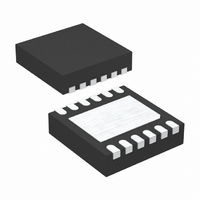
LTC4352IDD#PBF Linear Technology, LTC4352IDD#PBF Datasheet - Page 5

LTC4352IDD#PBF
Manufacturer Part Number
LTC4352IDD#PBF
Description
IC IDEAL DIODE CNTRL 12-DFN
Manufacturer
Linear Technology
Datasheet
1.LTC4352CMSPBF.pdf
(16 pages)
Specifications of LTC4352IDD#PBF
Applications
Redundant Power Supplies, Telecom Infrastructure
Fet Type
N-Channel
Number Of Outputs
1
Internal Switch(s)
No
Delay Time - On
250ns
Delay Time - Off
200ns
Voltage - Supply
2.9 V ~ 18 V
Current - Supply
1.4mA
Operating Temperature
-40°C ~ 85°C
Mounting Type
Surface Mount
Package / Case
12-DFN
Lead Free Status / RoHS Status
Lead free / RoHS Compliant
Available stocks
Company
Part Number
Manufacturer
Quantity
Price
pin FuncTions
V
pin to the power input side of the MOSFET. The low voltage
supply V
this pin is used to control the MOSFET gate.
V
from this pin to ground. When V
decoupling for an internal regulator that generates a 4.1V
supply. For applications where V
external supply voltage in the range 2.9V to 6V to this pin.
UV (Pin 3): Undervoltage Comparator Input. Connect this
pin to an external resistive divider from V
age at this pin falls below 0.5V, an undervoltage fault is
detected and the MOSFET is turned off. The comparator
has a built-in hysteresis of 5mV. Tie to V
OV (Pin 4): Overvoltage Comparator Input. Connect this
pin to an external resistive divider from V
age at this pin rises above 0.5V, an overvoltage fault is
detected and the MOSFET is turned off. The comparator
has a built-in hysteresis of 5mV. Tie to GND if unused.
STATUS (Pin 5): MOSFET Status Output. This pin is pulled
low by an open-drain output when the external MOSFET
is on. An internal 10µA current source pulls this pin up
to a diode below V
an external pull-up. Tie to GND or leave open if unused.
FAULT (Pin 6): Fault Output. This pin is pulled low by an
open-drain output when a fault occurs. This fault could
either be an undervoltage fault, an overvoltage fault, or
an open MOSFET fault. The external MOSFET is turned off
for undervoltage and overvoltage faults, while it is left on
for open MOSFET fault. An internal 10µA current source
CC
IN
(Pin 1): Voltage Sense and Supply Input. Connect this
(Pin 2): Low Voltage Supply. Connect a 0.1μF capacitor
CC
is generated from V
CC
. It may be pulled above V
IN
IN
. The voltage sensed at
≥ 2.9V, this pin provides
IN
< 2.9V, connect an
CC
IN
IN
if unused.
. If the volt-
. If the volt-
CC
using
pulls this pin up to a diode below V
above V
open if unused.
REV (Pin 7): Reverse Current Enable Input. Connect this
pin to GND for normal diode operation that blocks reverse
current. Driving this pin above 1V fully turns on the MOSFET
gate to allow reverse current. An internal 10µA current
source pulls this pin to GND.
OUT (Pin 8): Output Voltage Sense Input. Connect this
pin to the output side of the MOSFET. The voltage sensed
at this pin is used to control the MOSFET gate.
GND (Pin 9): Device Ground.
CPO (Pin 10): Charge Pump Output. Connect a capacitor
from this pin to the SOURCE pin. The value of this capaci-
tor is approximately 10x the gate capacitance (C
MOSFET switch. The charge stored on this capacitor is
used to pull-up the gate during a fast turn-on. Leave this
pin open if fast turn-on is not needed.
GATE (Pin 11): MOSFET Gate Drive Output. Connect this
pin to the gate of the external N-channel MOSFET switch.
An internal clamp limits the gate voltage to 6.1V above,
and a diode below SOURCE. During fast turn-on a 1.5A
pull-up charges GATE to CPO. During fast turn-off a 1.5A
pull-down discharges GATE to SOURCE.
SOURCE (Pin 12): MOSFET Gate Drive Return. Connect
this pin to the source of the external N-channel MOSFET
switch.
EXPOSED PAD (Pin 13, DD Package Only): Exposed pad
may be left open or connected to device ground.
CC
using an external pull-up. Tie to GND or leave
CC
. It may be pulled
LTC4352
ISS
) of the
4352fa
5


