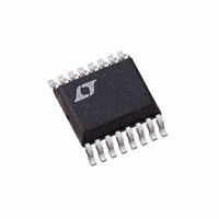
LTC1473LCGN Linear Technology, LTC1473LCGN Datasheet - Page 5

LTC1473LCGN
Manufacturer Part Number
LTC1473LCGN
Description
IC SWITCH DVR PWRPATH DUAL16SSOP
Manufacturer
Linear Technology
Series
PowerPath™r
Datasheet
1.LTC1473LCGNPBF.pdf
(16 pages)
Specifications of LTC1473LCGN
Applications
Handheld/Mobile Devices
Fet Type
N-Channel
Number Of Outputs
2
Internal Switch(s)
No
Delay Time - On
22µs
Delay Time - Off
1µs
Voltage - Supply
2.8 V ~ 9 V
Current - Supply
100µA
Operating Temperature
0°C ~ 70°C
Mounting Type
Surface Mount
Package / Case
16-SSOP
Power Switch Family
LTC1473L
Mounting
Surface Mount
Supply Current
100uA
Package Type
SSOP N
Operating Temperature (min)
0C
Operating Temperature (max)
70C
Operating Temperature Classification
Commercial
Pin Count
16
Lead Free Status / RoHS Status
Contains lead / RoHS non-compliant
Available stocks
Company
Part Number
Manufacturer
Quantity
Price
Company:
Part Number:
LTC1473LCGN
Manufacturer:
LT
Quantity:
10 000
Part Number:
LTC1473LCGN
Manufacturer:
LINEAR/凌特
Quantity:
20 000
Company:
Part Number:
LTC1473LCGN#PBF
Manufacturer:
Linear Technology
Quantity:
135
Part Number:
LTC1473LCGN#PBF
Manufacturer:
LINEAR/凌特
Quantity:
20 000
PI FU CTIO S
IN1 (Pin 1): Logic Input of Gate Drivers GA1 and GB1. IN1
is disabled when IN2 is high or DIODE is low. During
2-diode mode, asserting IN1 disables the fault timer
function.
IN2 (Pin 2): Logic Input of Gate Drivers GA2 and GB2. IN2
is disabled when IN1 is high or DIODE is low. During
2-diode mode, asserting IN2 disables the fault timer
function.
DIODE (Pin 3): “2-Diode Mode” Logic Input. Diode over-
rides IN1 and IN2 by forcing the two back-to-back
external N-channel MOSFET switches to mimic two di-
odes.
TIMER (Pin 4): Fault Timer. A capacitor connected from
this pin to GND programs the time the MOSFET switches
are allowed to be in current limit. To disable this function,
Pin 4 can be grounded.
V
1 F capacitor.
V
is intended only for driving the internal micropower gate
drive circuitry. Do not load this pin with any external
circuitry . Bypass this pin with at least 1 F.
Pin Function Table
PIN
1
2
3
4
5
6
7
8
9
10
11
12
13
14
15
16
+
GG
U
(Pin 5): Power Supply. Bypass this pin with at least a
(Pin 6): Gate Driver Supply. This high voltage supply
NAME
IN1
IN2
DIODE
TIMER
V
V
SW
GND
GB2
SAB2
GA2
SENSE
SENSE
GB1
SAB1
GA1
GG
+
U
–
+
DESCRIPTION
Logic Input of Gate Drivers GA1 and GB1
Logic Input of Gate Drivers GA2 and GB2
“2-Diode Mode” Logic Input
Fault Timer Programs Time in Current Limit
Power Supply
Gate Driver Supply
Switch Node of Internal Boost Switching Regulator
Ground
Switch Gate Driver for Switch B2
Source Return of Switch 2
Switch Gate Driver for Switch A2
Inrush Current Input, Low Side
Inrush Current Input, High Side
Switch Gate Driver for Switch B1
Source Return of Switch 1
Switch Gate Driver for Switch A1
U
SW (Pin 7): Open Drain of an Internal N-Channel MOSFET
Switch. This pin drives the bottom of the V
regulator inductor which is connected between this pin and
the V
GND (Pin 8): Ground.
GB2, GA2 (Pins 9, 11): Switch Gate Drivers. GA2 and GB2
drive the gates of the second back-to-back external
N-channel switches.
SAB2 (Pin 10): Source Return. The SAB2 pin is connected
to the sources of SW A2 and SW B2. A small pull-down
current source returns this node to 0V when the switches
are turned off.
SENSE
connected directly to the bottom (output side) of the low
valued resistor in series with the two input power selector
switch pairs, SW A1/B1 and SW A2/B2, for detecting and
controlling the inrush current into and out of the power
supply sources and the output capacitor.
SENSE
connected directly to the top (switch side) of the low
valued resistor in series with the two input power selector
switch pairs, SW A1/B1 and SW A2/B2, for detecting and
controlling the inrush current into and out of the power
supply sources and the output capacitor. Current limit is
invoked when (V
+
pin.
–
+
MIN
10.2
0.4
0.4
0.4
2.8
(Pin 12): Inrush Current Input. This pin should be
(Pin 13): Inrush Current Input. This pin should be
0
0
0
0
0
0
0
0
0
NOMINAL (V)
1.16
TYP
SENSE
1
0
1
1
+
MAX
– V
20
20
17
10
17
10
10
17
10
17
2
2
2
9
SENSE
–
– 0.3
– 0.3
– 0.3
– 0.3
– 0.3
– 0.3
– 0.3
– 0.3
– 0.3
– 0.3
– 0.3
– 0.3
– 0.3
– 0.3
– 0.3
MIN
) exceeds 0.2V.
0
ABSOLUTE MAX (V)
LTC1473L
GG
switching
MAX
10
20
20
20
10
20
10
10
20
10
20
7
7
7
5
0
5


