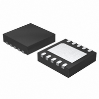
LTC4413EDD-2#TRPBF Linear Technology, LTC4413EDD-2#TRPBF Datasheet - Page 2

LTC4413EDD-2#TRPBF
Manufacturer Part Number
LTC4413EDD-2#TRPBF
Description
IC IDEAL DIODE DUAL 10-DFN
Manufacturer
Linear Technology
Datasheet
1.LTC4413EDD-1PBF.pdf
(16 pages)
Specifications of LTC4413EDD-2#TRPBF
Applications
Handheld/Mobile Devices
Fet Type
P-Channel
Number Of Outputs
2
Internal Switch(s)
Yes
Delay Time - On
11µs
Delay Time - Off
2µs
Voltage - Supply
2.5 V ~ 5.5 V
Current - Supply
40µA
Operating Temperature
-40°C ~ 85°C
Mounting Type
Surface Mount
Package / Case
10-DFN
Lead Free Status / RoHS Status
Lead free / RoHS Compliant
Available stocks
Company
Part Number
Manufacturer
Quantity
Price
ABSOLUTE MAXIMUM RATINGS
LTC4413-1/LTC4413-2
INA, INB, OUTA, OUTB, STAT,
ENBA, ENBB Voltage .................................... –0.3V to 6V
OVI, OVP Voltage ....................................... –0.3V to 13V
Operating Temperature Range .................–40°C to 85°C
PIN CONFIGURATION
ORDER INFORMATION
LEAD FREE FINISH
LTC4413EDD-1#PBF
LTC4413EDD-2#PBF
LEAD BASED FINISH
LTC4413EDD-1
LTC4413EDD-2
Consult LTC Marketing for parts specifi ed with wider operating temperature ranges.
For more information on lead free part marking, go to:
For more information on tape and reel specifi cations, go to:
ELECTRICAL CHARACTERISTICS
temperature range, otherwise specifi cations are at T
SYMBOL
V
UVLO
I
I
I
2
LTC4413-1
QF
QRIN
QRGND
IN
, V
OUT
PARAMETER
Operating Supply Range for Channel A or B V
UVLO Turn-On Rising Threshold
UVLO Turn-Off Falling Threshold
Quiescent Current in Forward Regulation,
Measured via GND
Current Drawn from or Sourced into IN
When V
Quiescent Current While in Reverse
Turn-Off, Measured via GND
EXPOSED PAD (PIN 11) IS GND, MUST BE SOLDERED TO PCB
OUT
ENBA
ENBB
GND
10-LEAD (3mm × 3mm) PLASTIC DFN
INA
INB
is Greater than V
T
JMAX
TAPE AND REEL
LTC4413EDD-1#TRPBF
LTC4413EDD-2#TRPBF
TAPE AND REEL
LTC4413EDD-1#TR
LTC4413EDD-2#TR
1
2
3
4
5
= 125°C, θ
DD PACKAGE
TOP VIEW
11
JA
IN
= 43°C/W
10
9
8
7
6
OUTA
STAT
NC
NC
OUTB
http://www.linear.com/leadfree/
PART MARKING
LCPP
LCPQ
PART MARKING
LCPP
LCPQ
CONDITIONS
Proper Operation
Max (V
Max (V
V
I
V
V
V
http://www.linear.com/tapeandreel/
INB
A
IN
INA
IN
INA
STAT
= 25°C. (Notes 2, 6)
and/or V
= 3.6V, V
= 0mA (Note 3)
= 3.6V, I
= V
= 0V
INA
INA
INB
The
, V
, V
= 0V, V
OUT
OUT
INB
INB
(Note 1)
INA
l
, V
, V
denotes the specifi cations which apply over the full operating
Must be in This Range for
= 100mA, V
= 5.5V (Note 6)
OUTA
OUTA
OUTB
LTC4413-2
Storage Temperature Range .................. –65°C to 125°C
Continuous Power Dissipation ..........................1500mW
(Derate 25mW/°C Above 70°C)
, V
, V
= V
OUTB
OUTB
PACKAGE DESCRIPTION
10-Lead (3mm × 3mm) Plastic DFN
10-Lead (3mm × 3mm) Plastic DFN
PACKAGE DESCRIPTION
10-Lead (3mm × 3mm) Plastic DFN
10-Lead (3mm × 3mm) Plastic DFN
OUTA
INB
)
)
= 0V,
= 5.5V,
EXPOSED PAD (PIN 11) IS GND, MUST BE SOLDERED TO PCB
ENBA
ENBB
10-LEAD (3mm × 3mm) PLASTIC DFN
GND
INA
INB
T
JMAX
1
2
3
4
5
l
l
l
l
l
= 125°C, θ
DD PACKAGE
TOP VIEW
11
MIN
2.5
1.7
–1
JA
= 43°C/W
10
9
8
7
6
TYP
2.5
40
28
TEMPERATURE RANGE
–40°C to 85°C
–40°C to 85°C
TEMPERATURE RANGE
–40°C to 85°C
–40°C to 85°C
OUTA
STAT
OVI
OVP
OUTB
MAX
2.45
5.5
4.5
58
36
441312fd
UNITS
μA
μA
μA
V
V
V


