LTC4355CDE#TRPBF Linear Technology, LTC4355CDE#TRPBF Datasheet - Page 5
LTC4355CDE#TRPBF
Manufacturer Part Number
LTC4355CDE#TRPBF
Description
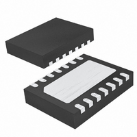
IC IDEAL DIODE-OR 14-DFN
Manufacturer
Linear Technology
Datasheet
1.LTC4355ISPBF.pdf
(20 pages)
Specifications of LTC4355CDE#TRPBF
Applications
-48V Dist Power Systems, AdvancedTCA ® Systems
Fet Type
N-Channel
Number Of Outputs
2
Internal Switch(s)
No
Delay Time - Off
300ns
Voltage - Supply
9 V ~ 80 V
Current - Supply
2mA
Operating Temperature
0°C ~ 70°C
Mounting Type
Surface Mount
Package / Case
14-DFN
Lead Free Status / RoHS Status
Lead free / RoHS Compliant
Delay Time - On
-
Available stocks
Company
Part Number
Manufacturer
Quantity
Price


PIN FUNCTIONS
Exposed Pad: Exposed pad may be left open or connected
to GND.
FUSEFLTx: Fuse Fault Outputs. Open-drain output that
pulls to GND when V
has blown open. Otherwise, this output is high impedance.
Connect to GND if unused.
GATEx: Gate Drive Outputs. The GATE pins pull high,
enhancing the N-channel MOSFET when the load cur-
rent creates more than 25mV of voltage drop across
the MOSFET. When the load current is small, the
gates are actively driven to maintain 25mV across the
MOSFET. If the reverse current develops more than
–25mV of voltage drop across a MOSFET, a fast pull-down
circuit quickly connects the GATE pin to the IN pin, turning
off the MOSFET. Limit the capacitance between the GATE
and IN pins to less than 0.1μF.
GND: Device Ground.
INx: Input Voltages and GATE Fast Pull-Down Returns. The
IN pins are the anodes of the ideal diodes and connect to the
sources of the N-channel MOSFETs. The voltages sensed
at these pins are used to control the source-drain voltages
across the MOSFETs and are used by the fault detection
circuits that drive the PWRFLT, FUSEFLT, and VDSFLT pins.
The GATE fast pull-down current is returned through the IN
pins. Connect these pins as close to the MOSFET sources
as possible. Connect to OUT if unused.
MONx: Input Supply Monitors. These pins are used to
sense the input supply voltages. Connect these pins to
external resistive dividers between the input supplies and
GND. If V
to GND. Connect to GND if unused.
MONx
falls below 1.23V, the PWRFLTx pin pulls
INx
< 3.5V, indicating that the fuse
NC: No Connection. Not internally connected. These
pins provide extra distance between high and low volt-
age pins.
OUT: Drain Voltage Sense and Positive Supply Input. OUT
is the diode-OR output of IN1 and IN2. It connects to the
common drain connection of the N-channel MOSFETs. The
voltage sensed at this pin is used to control the source-
drain voltages across the MOSFETs and is used by the
fault detection circuits that drive the PWRFLT and VDSFLT
pins. The LTC4355 is powered from the OUT pin.
PWRFLTx: Power Fault Outputs. Open-drain output
that pulls to GND when V
the forward voltage across the MOSFET exceeds
ΔV
forward voltage across the MOSFET is less than
ΔV
if unused.
SET: ΔV
to GND, to a 100k resistor connected to GND, or leaving
SET open confi gures the ΔV
threshold to 250mV, 500mV, or 1.5V, respectively. When the
voltage across a MOSFET exceeds ΔV
pin and at least one of the PWRFLT pins pull to GND.
VDSFLT: MOSFET Fault Output. Open-drain output that
pulls to GND when the forward voltage across either
MOSFET exceeds ΔV
pulls low to indicate which MOSFET’s forward voltage drop
exceeds ΔV
Connect to GND if unused.
SD(FLT)
SD(FLT)
SD(FLT)
, PWRFLTx is high impedance. Connect to GND
. When V
SD(FLT)
Threshold Confi guration Input. Tying SET
. Otherwise, this pin is high impedance.
SD(FLT)
MONx
. PWRFLT1 or PWRFLT2 also
SD(FLT)
MONx
is above 1.23V and the
falls below 1.23V or
forward voltage fault
SD(FLT)
LTC4355
, the VSDFLT
4355fe
5
Related parts for LTC4355CDE#TRPBF
Image
Part Number
Description
Manufacturer
Datasheet
Request
R

Part Number:
Description:
IC IDEAL DIODE-OR 14-DFN
Manufacturer:
Linear Technology
Datasheet:

Part Number:
Description:
Positive High Voltage Ideal Diode-OR with Input Supply and Fuse Monitors
Manufacturer:
LINER [Linear Technology]
Datasheet:

Part Number:
Description:
CD ROM LINEARVIEW DATASHEETS
Manufacturer:
Linear Technology

Part Number:
Description:
Standalone Linear Li-Ion Battery Charger with Thermal Regulation in ThinSOT
Manufacturer:
Linear Technology Corporation
Datasheet:
Part Number:
Description:
Low noise, high frequency, 8th order linear phase lowpass filter
Manufacturer:
Linear Technology Corporation
Datasheet:
Part Number:
Description:
Manufacturer:
Linear Technology Corporation
Datasheet:
Part Number:
Description:
Manufacturer:
Linear Technology Corporation
Datasheet:
Part Number:
Description:
Manufacturer:
Linear Technology Corporation
Datasheet:
Part Number:
Description:
Manufacturer:
Linear Technology Corporation
Datasheet:
Part Number:
Description:
Manufacturer:
Linear Technology Corporation
Datasheet:
Part Number:
Description:
Manufacturer:
Linear Technology Corporation
Datasheet:
Part Number:
Description:
Manufacturer:
Linear Technology Corporation
Datasheet:
Part Number:
Description:
Dual and Quad, JFET Input Precision High Speed Op Amps
Manufacturer:
Linear Technology Corporation
Datasheet:
Part Number:
Description:
Manufacturer:
Linear Technology Corporation
Datasheet:
Part Number:
Description:
1, 2, 6 and 8 Channel, 10-Bit Serial I/O Data Acquisition Systems
Manufacturer:
Linear Technology Corporation
Datasheet: