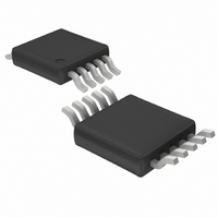
LTC4416IMS-1#PBF Linear Technology, LTC4416IMS-1#PBF Datasheet - Page 9

LTC4416IMS-1#PBF
Manufacturer Part Number
LTC4416IMS-1#PBF
Description
IC CNTRLR POWERPATH 10-MSOP
Manufacturer
Linear Technology
Series
PowerPath™r
Datasheet
1.LTC4416EMS-1PBF.pdf
(12 pages)
Specifications of LTC4416IMS-1#PBF
Applications
Battery Backup, Industrial/Automotive, High Current Switch
Fet Type
P-Channel
Number Of Outputs
2
Internal Switch(s)
No
Delay Time - On
60µs
Delay Time - Off
30µs
Voltage - Supply
3.6 V ~ 36 V
Current - Supply
130µA
Operating Temperature
-40°C ~ 125°C
Mounting Type
Surface Mount
Package / Case
10-MSOP, Micro10™, 10-uMAX, 10-uSOP
Lead Free Status / RoHS Status
Lead free / RoHS Compliant
Available stocks
Company
Part Number
Manufacturer
Quantity
Price
APPLICATIO S I FOR ATIO
This configuration would be used where V1 is a 12V power
supply and the V2 power supply is a 4-cell Li-Ion battery
pack. When V1 is 12V, E2 disables the V2 source from
being connected to V
G2 to V2, H2 is open circuit. E1 is connected to a voltage
greater than the V
V
input. The LTC4416 takes its power from the higher of V1,
V2 and V
to V
When V1 drops below 9V, the H2 pin closes to GND, G2
drops to a V
age level. V2 will supply current to V
10.8V. The H1 output will be open until the E1 input drops
below the V
The V1 V
The V1 V
V1 is Greater Than V2
Figure 3 illustrates the external resistor configuration for
this case.
This configuration would be used where V1 is a 12V power
supply and the V2 power supply is a 3-cell Li-Ion battery
pack. When V1 is 16V, E1 enables the V1 source as being the
primary supply, thus disabling the V2 supply since V1 > V2.
When E1 > V
shut completely off by grounding the H1 input and forcing
E2 > V
V1, V2 and V
V1 to V
S
output can be shut completely off by grounding the E1
V
V
S
FAIL
RESTORE
until the V1 supply drops below 9V.
REF
S
=
=
S
until the V1 supply drops below 12V.
FAIL
RESTORE
. The LTC4416 takes its power from the higher of
. This configuration will provide power from V1
1 222
V
.
REF
ETH
REF
CLAMP
S
=
=
is determined by:
. This configuration will provide power from
1 222
, the H1 output is open. The V
V
voltage level.
•
.
ETH
V
R A R c
REF
is determined by:
•
below V2 and G1 rises to the V
2
U
158
•
R c
V
to keep the V1 to V
S
(
+
2
R A
•
through Q2A and Q2B by forcing
24 9k k
k
15 5 8
2
+
2
U
.
R c R E
24 9
+
k
2
24 9 105
(
+
.
R c R E
(
.
k
2
24 9 105
k
2
= 8 98
.
W
S
.
2
until V1 rises above
k
S
k
)
V
)
path active. The
S
k
output can be
)
=
U
10 81
S
.
volt-
V
When V1 drops below 12V, the H1 pin closes to GND,
G2 drops to a V
voltage level. V2 will supply current to V
above 13.5V. The H2 output will be shorted to GND until
the E2 input goes above the V
The V1 V
The V1 V
Load Sharing
Figure 4 illustrates the configuration for this case.
This configuration would be used where V1 and V2 are
relatively the same voltage. In this case the LTC4416 acts
as two interconnected ideal diode controllers. V
supplied by the higher of the two supplies, V1 and V2. If
V1 and V2 are exactly the same, then 50% of the current
for V
GND
V1
V2
V
V
FAIL
RESTORE
S
V1 = 13.5V (RESTORE)
will be supplied by each supply. As the two supplies
V1 = 12V (FAIL)
V2 = 10.8V
=
=
FAIL
RESTORE
R1D
187k
1 222
V
.
ETH
=
=
is determined by:
1 222
R1A
221k
V
R1C
24.9k
•
.
LTC4416/LTC4416-1
CLAMP
V
ETH
R A R c
is determined by:
•
1
221
R c
•
V
+
(
1
R A
•
PRIMARY SUPPLY
E1
GND
E2
H2
H1
below V2 and G1 rises to the V1
24 9k k
BACKUP SUPPLY
k
22 2 1
1
Figure 3
+
1
LTC4416
.
R c R D
24 9
+
k
1
24 9 187
(
+
.
R c R D
REF
(
.
1
k
24 9 187
V1
G1
V
G2
V2
1
k
= 12 07
S
voltage level.
.
1
k
.
SUP75P03_07
)
k
)
SUP75P03_07
S
V
Q1
Q3
until V1 rises
k
)
=
Q2
13 51
S
will be
4416 F03
.
4416fa
V
V
S


