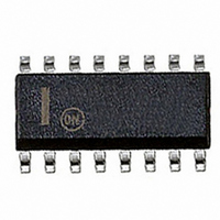
NCP1651DR2 ON Semiconductor, NCP1651DR2 Datasheet - Page 20

NCP1651DR2
Manufacturer Part Number
NCP1651DR2
Description
IC CTRLR PWR FACTOR SGL 16SOIC
Manufacturer
ON Semiconductor
Specifications of NCP1651DR2
Mode
Continuous Conduction (CCM), Discontinuous Conduction (DCM)
Frequency - Switching
250kHz
Current - Startup
8.5mA
Voltage - Supply
10 V ~ 18 V
Operating Temperature
-40°C ~ 125°C
Mounting Type
Surface Mount
Package / Case
16-SOIC (3.9mm Width)
Start-up Supply Current
5.5/8.5mA
Switching Freq
110kHz
Operating Supply Voltage (min)
-3V
Operating Supply Voltage (max)
18V
Operating Temp Range
-40C to 125C
Operating Temperature Classification
Automotive
Package Type
SOIC
Pin Count
16
Mounting
Surface Mount
Switching Frequency
110 KHz
Maximum Operating Temperature
+ 125 C
Mounting Style
SMD/SMT
Minimum Operating Temperature
- 40 C
Lead Free Status / RoHS Status
Contains lead / RoHS non-compliant
Other names
NCP1651DR2OS
Available stocks
Company
Part Number
Manufacturer
Quantity
Price
Part Number:
NCP1651DR2G
Manufacturer:
ON/安森美
Quantity:
20 000
The ramp signal injected can be calculated by the following
formula:
Where:
V
R
Oscillator
the switching frequency, as well as sets the gain for the
multipliers. Both the frequency and the peak- -to- -peak
amplitude are important parameters.
capacitor on the C
200 mA and is trimmed to maintain an accurate, repeatable
frequency. Discharge is accomplished by grounding the C
pin with a saturated transistor. A hysteretic comparator
monitors that ramp signal and is used to switch between the
current source and discharge transistor. While the cap is
charging, the comparator has a reference voltage of
4.0 volts. When the ramp reaches that voltage, the
comparator switches from the charging circuit to the
discharge circuit, and its reference changes from 4.0 to ~0.5
volts (overshoot and delays will allow the valley voltage to
reach 0 volts).
capacitor is:
Where C
this could affect the accuracy of the frequency as well as that
of the multipliers which use the ramp signal. Any use of this
signal should incorporate a high impedance buffer.
ramp
RC
The current mirror is designed with a 1:1.6 current ratio.
The oscillator generates the sawtooth ramp signal that sets
The oscillator uses a current source for charging the
The relationship between the frequency and timing
It is important not to load the capacitor on this pin, since
Oscillator
= Ramp compensation resistor (kΩ)
= Peak injected current signal (4 V)
Figure 35. Ramp Compensation Circuit
T
V ramp =
is in pF and f is in kHz.
+
--
T
i
1.6 Vosc pk 16 k
pin. The charge rate is approximately
C T = 47, 000∕f
4
Ramp Compensation
R
R RC
RC
1.6
i
=
Current
16 k
Sense
102, 400
Amp
R RC
Comparator
AC Ref
Buffer
http://onsemi.com
(eq. 1)
PWM
+
--
T
20
voltages, the NCP1651 is not designed to be synchronized
to the frequency of another oscillator.
Average Current Compensation
rectified sinewave. The amplifier is a unity gain amplifier,
with a voltage divider on the output that attenuates the signal
by a factor of 0.75. This scaled down fullwave rectified
sinewave is summed with the low frequency current signal
out of the current sense amplifier.
non- -inverting input to the AC error amplifier, which is the
output of the reference multiplier. Since there is a hard limit
of 4.5 volts at the non- -inverting input, the sum of the line
voltage plus the current cannot exceed this level.
265 vac, which is a range of 3.1:1. The output of the Current
Compensation amplifier will change by this amount to allow
the maximum current to vary inversely to the line voltage.
AC Error Amplifier
This amplifier forces a signal which is the sum of the current
and input voltage to equal the AC reference signal from the
reference multiplier.
amplifiers in that the output is a high impedance with a
controlled voltage- -to- -current gain. This amplifier has a
nominal gain of 100 umhos (or 0.0001 amps/volt). This
means that an input voltage differential of 10 mv would
cause the output current to change by 1.0 mA. Its maximum
output current is 30 mA.
Current Sense Amplifier
with a differential input. It consists of a differential input
stage, a high frequency current mirror (PWM output) and a
low frequency current mirror (AC error amp output).
5
Due to the required accuracy of the peak and valley ramp
The input signal to this amplifier is the input fullwave
The sum of these signals must equal the signal at the
A typical universal input design operates from 85 to
The AC error amplifier is a transconductance amplifier.
Transconductance amplifiers differ from voltage
The current sense amplifier is a wide bandwidth amplifier
3 k
I
S+
Figure 36. Current Sense Amplifier
3 k
i
CURRENT
1
MIRROR
i
1
30 k
i
1
6
I
avg fltr
LEB
+
--
PWM
7
CURRENT
MIRROR
i
2
I
avg
Error
Amp
AC
i
2


