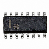
MC33368D ON Semiconductor, MC33368D Datasheet - Page 9

MC33368D
Manufacturer Part Number
MC33368D
Description
IC POWER FACTOR CTRLR HV 16-SOIC
Manufacturer
ON Semiconductor
Series
GreenLine™r
Datasheet
1.MC33368DR2G.pdf
(16 pages)
Specifications of MC33368D
Mode
Critical Conduction (CRM)
Current - Startup
16mA
Voltage - Supply
10 V ~ 16 V
Operating Temperature
-25°C ~ 125°C
Mounting Type
Surface Mount
Package / Case
16-SOIC (3.9mm Width)
Maximum Operating Temperature
+ 125 C
Mounting Style
SMD/SMT
Minimum Operating Temperature
- 25 C
Lead Free Status / RoHS Status
Contains lead / RoHS non-compliant
Frequency - Switching
-
Lead Free Status / Rohs Status
Lead free / RoHS Compliant
Available stocks
Company
Part Number
Manufacturer
Quantity
Price
Part Number:
MC33368D
Manufacturer:
ON/安森美
Quantity:
20 000
Company:
Part Number:
MC33368DG
Manufacturer:
ON Semiconductor
Quantity:
7
Part Number:
MC33368DR2
Manufacturer:
MOTOROLA/摩托罗拉
Quantity:
20 000
Company:
Part Number:
MC33368DR2G
Manufacturer:
ON
Quantity:
1 570
Part Number:
MC33368DR2G
Manufacturer:
MOTOROLA/摩托罗拉
Quantity:
20 000
In this manner, the SMPS switching transistors are operated
at very low duty cycles, preventing their destruction. If the
short circuit fault is removed, the power supply system will
turn on by itself in a normal startup mode after the restart
delay has timed out.
Output Switching Frequency Clamp
inductor in the critical mode. That is, the inductor current
ramps to a peak value, ramps down to zero, then
immediately begins ramping positive again. The peak
current is programmed by the multiplier output within the
IC. As the input voltage haversine declines to near zero, the
output switch on- -time becomes constant, rather than going
to zero because of the small integrated dc voltage at Pin 5
caused by C2, R3 and R5. Because of this, the average line
current does not exactly follow the line voltage near the zero
crossings. The Output Switching Frequency Clamp
remedies this situation to improve power factor and
minimize EMI generated in this operating region. The
values of R10 and C7, as shown in Figure 16, program a
minimum off- -time in the frequency clamp which overrides
the zero current detect signal, forcing a minimum off- -time.
This allows discontinuous conduction operation of the boost
inductor in the zero crossing region, and the average line
current more nearly follows the voltage. The Output
In normal operation, the MC33368 operates the boost
http://onsemi.com
9
Switching Frequency Clamp function can be disabled by
connecting the FC input, Pin 13, to the V
values of R10 and C7, should be chosen so that t
+ t
frequency clamp input is less than 2.0 V. When the output
drive is high, C7 is discharged through an internal 100 mA
current source. When the output drive switches low, C7 is
charged through R10. The drive output is inhibited until the
voltage across C7 reaches 2.0 V, establishing a minimum
off- -time where:
Output
specifically designed for direct drive of power MOSFETs.
The Gate Output is capable of up to 1500 mA peak current
with a typical rise and fall time of 50 ns with a 1.0 nF load.
Additional internal circuitry has been added to keep the Gate
Output in a sinking mode whenever the Undervoltage
Lockout is active. This characteristic eliminates the need for
an external gate pull- -down resistor. The totem- -pole output
has been optimized to minimize cross- -conduction current
during high speed operation.
For best results, the minimum off- -time, determined by the
The IC contains a CMOS output driver that was
(off)fc
t
(off)fc
. Output drive is inhibited when the voltage at the
= − R10 C7 log e
1 −
CC
supply Pin 12.
V
CC
2
s(min)
= t
(on)


