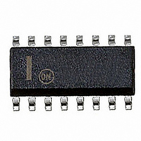
NCP1605DR2G ON Semiconductor, NCP1605DR2G Datasheet - Page 26

NCP1605DR2G
Manufacturer Part Number
NCP1605DR2G
Description
IC PFC CONTROLLER CCM/DCM 16SOIC
Manufacturer
ON Semiconductor
Datasheet
1.NCP1605ADR2G.pdf
(32 pages)
Specifications of NCP1605DR2G
Mode
Continuous Conduction (CCM), Discontinuous Conduction (DCM)
Frequency - Switching
250kHz
Current - Startup
12mA
Voltage - Supply
10 V ~ 20 V
Operating Temperature
0°C ~ 125°C
Mounting Type
Surface Mount
Package / Case
16-SOIC (3.9mm Width)
Output Voltage Range
10 V to 20 V
Input Voltage Range
- 0.3 V to + 9 V
Power Dissipation
550 mW
Operating Temperature Range
- 40 C to + 125 C
Mounting Style
SMD/SMT
Lead Free Status / RoHS Status
Lead free / RoHS Compliant
Available stocks
Company
Part Number
Manufacturer
Quantity
Price
Part Number:
NCP1605DR2G
Manufacturer:
ON/安森美
Quantity:
20 000
Startup Sequence / V
mains outlet, the internal current source starts charging the
V
is enabled whenever V
typically). When V
15 V for the NCP1605, 10.5 V for the NCP1605A), the
current source turns off and the circuit starts pulsing.
controller and some auxiliary supply must take over before
V
below which the circuit stops pulsing.
exceeds V
V
the NCP1605A) prevents erratic operation as the V
crosses the V
structure (the V
Inductor
CC
CC
CC
Current
At the moment when the PFC stage is plugged to the
The energy stored by the V
Hence, the circuit starts operating when the V
Figure 67 shows the internal arrangement of this
Signal
Clock
Clock
Edge
OFF. The hysteresis (6 V for the NCP1605, 1.5 V for
Discontinuous Mode
drops below V
capacitor. More generally, the startup current source
Set
CC
Figure 65. Oscillator Timing Diagram
(When high, ”UVLO” indicates that the circuit is not properly fed and it sets the Fault latch to turn off the circuit)
ON and stops pulsing when V
CC
CC
ON threshold.
turn on threshold of Figure 67 is that of
CC
CC
OFF (9 V, typically), that is, the level
CC
exceeds the V
Figure 67. The Current Source brings V
CC
Management
drops below V
15 V / 7 V
CC
Critical Mode
capacitor serves to feed the
9 V
CC
ON level (typically
CC
CC
+
-
+
-
HVCS_ON
drops below
STUP (7 V,
CC
voltage
UVLO
http://onsemi.com
Time
CC
Osc/Sync
15 mA / 0
26
CC
the NCP1605). One can note that the startup current source
is on during the V
the time. Hence, it spends no power during the PFC stage
operation and in particular, in light load conditions. That is
why the NCP1605(A) helps meet the most stringent
standby requirements.
Remarks:
•
•
Some circuitry (not represented in Figure 67) limits
the HV pin current below 1 mA if the V
nearly below 1 V. This protects the circuit when the
V
capability (around 15 mA) is obtained when V
exceeds about 1 V.
The circuit is also kept off when the startup current
source is on to make a clear distinction between the
V
“HVCS_ON” signal on block diagram).
above 15 V and then Turns Off
200 mA
CC
CC
V
GND
100 mA
HV
16
10
CC
9
V
pin is accidentally grounded. The full current
charge phase and the operating sequence (refer to
OSC
Figure 66. Oscillator / Synchronization Block
H/V
+
Cvcc
+
-
COMP_OSC
OSC
HV
CC
L
charging phase and off for the rest of
Auxiliary
Winding
Generation
S
R
CLOCK
Latch
delay
Q
Ct_OK
CLK
CC
voltage is
(”DT” is high
during the
dead−time)
DT
(PWM latch
SET input)
CC


