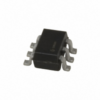
MIC2005-1.2YM6 TR Micrel Inc, MIC2005-1.2YM6 TR Datasheet - Page 15

MIC2005-1.2YM6 TR
Manufacturer Part Number
MIC2005-1.2YM6 TR
Description
IC DISTRIBUTION SW 1.2A SOT23-6
Manufacturer
Micrel Inc
Type
High Side Switchr
Specifications of MIC2005-1.2YM6 TR
Number Of Outputs
1
Rds (on)
100 mOhm
Internal Switch(s)
Yes
Current Limit
1.2A
Voltage - Input
2.5 ~ 5.5 V
Operating Temperature
-40°C ~ 85°C
Mounting Type
Surface Mount
Package / Case
SOT-23-6
Short Circuit Current Limit
1.6A
Input Voltage Range
2.5 to 5.5V
Number Of Switches
Single
Operating Temp Range
-40C to 85C
Operating Temperature Classification
Industrial
Mounting
Surface Mount
Pin Count
6
Package Type
SOT-23
Lead Free Status / RoHS Status
Lead free / RoHS Compliant
Other names
576-2589-2
MIC2005-1.2YM6 TR
MIC2005-1.2YM6TR
MIC2005-1.2YM6TR
MIC2005-1.2YM6 TR
MIC2005-1.2YM6TR
MIC2005-1.2YM6TR
January 2008
Supply Filtering
A 0.1µF to 1µF bypass capacitor positioned close to the
V
practice
MIC2005/2015. This will control supply transients and
ringing. Without a bypass capacitor, large current surges
or an output short may cause sufficient ringing on V
(from supply lead inductance) to cause erratic operation
of MIC2005/2015’s control circuitry. Good quality, low
ESR capacitors, such as Panasonic’s TE or ECJ series,
are suggested.
When bypassing with capacitors of 10µF and up, it is
good practice to place a smaller value capacitor in
parallel with the larger to handle the high frequency
components of any line transients. Values in the range
of 0.01µF to 0.1µF are recommended. Again, good
quality, low ESR capacitors should be chosen.
Power Dissipation
Power dissipation depends on several factors such as
the load, PCB layout, ambient temperature, and supply
voltage. Calculation of power dissipation can be
accomplished by the following equation:
To relate this to junction temperature, the following
equation can be used:
Where: T
In normal operation MIC2005/2015’s Ron is low enough
that no significant I2R heating occurs. Device heating is
most often caused by a short circuit, or very heavy load,
when a significant portion of the input supply voltage
appears across MIC2005/2015’s power MOSFET.
Under these conditions the heat generated will exceed
the package and PCB’s ability to cool the device and
thermal limiting will be invoked.
In Figure 10 die temperature is plotted against I
assuming a constant case temperature of 85°C. The
IN
and GND pins of MIC2005/2015 is both good design
T
R
P
T
A
D
J
θ(J-A)
= ambient temperature
=
=
J
P
R
is the thermal resistance of the package
and
= junction temperature,
D
DS(ON)
×
R
θ
required
(J
×
-
A)
(
I
OUT
+
T
A
)
2
for
proper
operation
OUT
of
IN
15
plots also assume a worst case R
temperature of 135°C. Under these conditions it is clear
that an SOT-23 packaged device will be on the verge of
thermal shutdown, typically 140°C die temperature,
when operating at a load current of 1.25A. For this
reason
MIC2005/2015s for any design intending to supply
continuous currents of 1A or more.
Figure 10 assumes no backside contact is made to the
thermal pad provided on the MLF package. For optimal
performance at higher current levels, or in higher
temperature environments, thermal contact with the
PCB and the exposed power paddle on the back side of
the MLF package should be made. This significantly
reduces the package’s thermal resistance thereby
extending the MIC2005/2015’s operating range. It
should be noted that this backside paddle is electrically
active and is connected to the MIC2005/2015’s GND
pin.
160
140
120
100
80
60
40
20
0
we
0.20 0.40 0.60 0.80 1.00 1.20 1.40 1.60 1.80 2.00
Figure 10. Die Temperature vs. I
Die Temperature vs. Iout for Tcase = 85°C
recommend
Iout - Amps
using
ON
of 140 mΩ at a die
MLF
M9999-011708-A
SOT-23
MLF
(408) 944-0800
OUT
packaged


