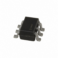
MIC2016-1.2YM6 TR Micrel Inc, MIC2016-1.2YM6 TR Datasheet - Page 25

MIC2016-1.2YM6 TR
Manufacturer Part Number
MIC2016-1.2YM6 TR
Description
IC DISTRIBUTION SW 1.2A SOT23-6
Manufacturer
Micrel Inc
Type
High Side Switchr
Datasheet
1.MIC2009YM6_TR.pdf
(29 pages)
Specifications of MIC2016-1.2YM6 TR
Number Of Outputs
1
Rds (on)
100 mOhm
Internal Switch(s)
Yes
Current Limit
1.2A
Voltage - Input
2.5 ~ 5.5 V
Operating Temperature
-40°C ~ 85°C
Mounting Type
Surface Mount
Package / Case
SOT-23-6
Lead Free Status / RoHS Status
Lead free / RoHS Compliant
Other names
576-2594-2
MIC2016-1.2YM6 TR
MIC2016-1.2YM6TR
MIC2016-1.2YM6TR
MIC2016-1.2YM6 TR
MIC2016-1.2YM6TR
MIC2016-1.2YM6TR
C
An
capacitance is a reduction in the MIC20X5 – 20X8’s
ability to quickly limit current transients or surges. A
sufficiently large capacitance can prevent both the
primary and secondary current limits from acting in time
to prevent damage to the MIC20X5 – 20X8 or the
system from a short circuit fault. For this reason, the
upper limit on the value of C
Variable Under Voltage Lock Out (VUVLO)
Only parts in bold have VUVLO pin and functionality.
Power conscious systems, such as those implementing
ACPI, will remain active even in their low power states
and may require the support of external devices through
both phases of operation. Under these conditions, the
current allowed these external devices may vary
according to the system’s operating state and as such
require dual current limits on their peripheral ports. The
MIC20X6 is designed for systems demanding two
primary current limiting levels but without the use of a
control signal to select between current limits.
To better understand how the MIC20X6 provides this,
imagine a system whose main power supply supports
heavy loads during normal operation, but in sleep mode
is reduced to only few hundred milliamps of output
current. In addition, this system has several USB ports
which must remain active during sleep. During normal
operation, each port can support a 500mA peripheral,
but in sleep mode their combined output current is
limited to what the power supply can deliver minus
whatever the system itself is drawing.
If a peripheral device is plugged in which demands more
current than is available, the system power supply will
sag, or crash. The MIC20X6 prevents this by monitoring
both the load current and V
when the power supply can source plenty of current, the
MIC20X6 will support any load up to its factory
February 2011
SLEW
2003
2013
Micrel, Inc.
Figure 8. C
unavoidable
’s effect on I
2004
2014
0.014
0.012
0.008
0.006
0.004
0.002
0.01
SLEW
14
12
10
vs. External C
0
6
4
2
0
8
2005X
2015
0 0.5 1 1.5 2 2.5 3 3.5 4 4.5
0
LIMIT
vs. Turn-On, Delay and Rise TImes
Typical Turn-on Times
0
consequence
0
C
2006
2016
0
SLEW
SLEW
SLEW
0
IN
. During normal operation,
0
(nF)
is 4nF.
Capacitance
2007
2017
0
T
ON
0
of
T
T
DELAY
RISE
0
2008
2018
adding
0
2009X
2019X
C
SLEW
25
programmed current limit. When the weaker, standby
supply is in operation, the MIC20X6 monitors V
shut off its output should V
value. This predetermined voltage is user programmable
and set by the selection of the resistor divider driving the
VUVLO pin.
To prevent false triggering of the VUVLO feature, the
MIC20X6 includes a delay timer to blank out momentary
excursions below the VUVLO trip point. If V
below the VUVLO trip point for longer than 32ms
(typical), then the load is disengaged and the MIC20X6
will wait 128ms before reapplying power to the load. If
V
will be powered for the 32ms blanking period and then
again disengaged. This is illustrated in the scope plot
below. If V
MIC20X6 resumes normal operation.
VUVLO and Kickstart™ operate independently in the
MIC2016. If the high current surge allowed by
Kickstart™ causes V
for more than 32ms, VUVLO will disengage the load
even though the Kickstart™ timer has not timed out.
Calculating VUVLO Resistor Divider Values
The VUVLO feature is designed to keep the internal
switch off until the voltage on the VUVLO pin is greater
than 0.25V. A resistor divider network connected to the
VUVLO and VIN pins is used to set the input trip voltage
V
minimize the load on the input supply I
of R1 sets the trip voltage V
IN
TRIP
remains below the VUVLO trip point, then the load
Supply
, see Figure 10. The value of R2 is chosen to
Input
I
IN_LOAD
Figure 10. VUVLO Application Circuit
IN
+
Figure 9. VUVLO Operation
remains above the VUVLO trip point
IN
to dip below the VUVLO trip point
R1
R2
IN
TRIP
dip below a predetermined
VIN
VUVLO
.
MIC20X6
VOUT
MIC20xx Family
DIV
M9999-020311-D
and the value
IN
IN
and will
+
stays


