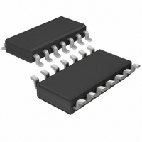
LTC1314CS#TRPBF Linear Technology, LTC1314CS#TRPBF Datasheet - Page 6

LTC1314CS#TRPBF
Manufacturer Part Number
LTC1314CS#TRPBF
Description
IC PCMCIA SWITCHNG MATRIX 14SOIC
Manufacturer
Linear Technology
Type
PCMCIA/Cardbus Switchr
Datasheet
1.LTC1314CSPBF.pdf
(12 pages)
Specifications of LTC1314CS#TRPBF
Number Of Outputs
1
Rds (on)
1.2 Ohm
Internal Switch(s)
Yes
Current Limit
120mA
Voltage - Input
3 ~ 5.5 V
Operating Temperature
0°C ~ 70°C
Mounting Type
Surface Mount
Package / Case
14-SOIC (3.9mm Width), 14-SOL
Lead Free Status / RoHS Status
Lead free / RoHS Compliant
Available stocks
Company
Part Number
Manufacturer
Quantity
Price
SWITCHI G TI E WAVEFOR S
LTC1314/LTC1315
APPLICATIONS
PCMCIA VPP control is easily accomplished using the
LTC1314 or LTC1315 switching matrix. Two control bits
(LTC1314) or four control bits (LTC1315) determine the
output voltage and standby/operate mode conditions. Out-
put voltages of 0V, V
impedance state are available. When either the high imped-
ance or low voltage (0V) conditions are selected, the device
switches into “sleep” mode and draws 0.1 A of current
from the V
The LTC1314/LTC1315 are low resistance power MOSFET
switching matrices that operate from the computer system
main power supply. Device power is obtained from V
which is 5V 0.5V. The gate drives for the NFETs (both
internal and external) are derived from internal charge
pumps, therefore VPP
to VPP
mine the output voltage and device mode.
Flash Memory Card VPP Power Considerations
PCMCIA compatible flash memory cards require tight
regulation of the 12V VPP programming supply to ensure
that the internal flash memory circuits are never subjected
to damaging conditions. Flash memory circuits are typi-
6
OUT
VPP
OUT
DD
. Internal break-before-make switches deter-
U
supply.
VPP
VCC
GND
EN0
EN1
IN
IN
U
NOTE: 1 F CAPACITOR CONNECTED ON BOTH VPP
CCIN
IN
W
is only required when it’s switched
INFORMATION
U
(3.3V or 5V), VPP
t
1
W
t
3
IN
t
4
W
, or a high
U
IN
t
AND V
DD
6
,
CCIN
PINS AT TIMING TEST
cally rated with an absolute maximum of 13.5V and VPP
must be maintained at 12V 5% under all possible load
conditions during erase and program cycles. Undervoltage
can decrease specified flash memory reliability and over-
voltage can damage the device.
V
Figures 1 and 2 show the approach that is very space and
power efficient. The LTC1314/LTC1315 used in conjunc-
tion with the LT1301 DC/DC converter, provide complete
power management for a PCMCIA card slot. The LTC1314/
LTC1315 and LT1301 combination provides a highly effi-
cient, minimal parts count solution. These circuits are
especially good for applications that are adding a PCMCIA
socket to existing systems that currently have only 5V or
3.3V available.
The LTC1314 drives three N-channel (LTC1315 six
N-channel) MOSFETs that provide V
ing. On-chip charge pumps provide the necessary voltage
to fully enhance the switches. With the charge pumps on-
chip, the MOSFET drive is available without the need for a
12V supply. The LTC1314/LTC1315 provide a natural
break-before-make action and smooth transitions due to
t
2
CC
Switch Driver and VPP Switch Matrix
t
5
Hi-Z
t
7
LTC1314 • SW
CC
pin power switch-


