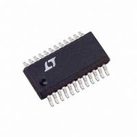
LTC1315CG#PBF Linear Technology, LTC1315CG#PBF Datasheet - Page 8

LTC1315CG#PBF
Manufacturer Part Number
LTC1315CG#PBF
Description
IC PCMCIA SWITCHNG MATRIX 24SSOP
Manufacturer
Linear Technology
Type
PCMCIA/Cardbus Switchr
Datasheet
1.LTC1314CSPBF.pdf
(12 pages)
Specifications of LTC1315CG#PBF
Number Of Outputs
1
Rds (on)
1.2 Ohm
Internal Switch(s)
Yes
Current Limit
120mA
Voltage - Input
3 ~ 5.5 V
Operating Temperature
0°C ~ 70°C
Mounting Type
Surface Mount
Package / Case
24-SSOP
Lead Free Status / RoHS Status
Lead free / RoHS Compliant
Available stocks
Company
Part Number
Manufacturer
Quantity
Price
APPLICATIONS
LTC1314/LTC1315
8
the asymmetrical turn-on and turn-off of the MOSFETs.
The LT1301 switching regulator is in shutdown mode and
consumes only 10 A until the VPP pins require 12V.
The VPP switching is accomplished by a combination of
the LTC1314/LTC1315 and LT1301. The LT1301 is in
shutdown mode to conserve power until the VPP pins
require 12V. When the VPP pins require 12V, the LT1301
is activated and the LTC1314/LTC1315’s internal switches
route the VPP
capable of delivering 12V at 120mA maintaining high
efficiency. The LTC1314/LTC1315’s break-before-make
and slope-controlled switching will ensure that the output
voltage transition will be smooth, of moderate slope, and
without overshoot. This is critical for flash memory prod-
ucts to prevent damaging parts from overshoot and
ringing exceeding the 13.5V device limit.
IN
(MAY BE FROM
pin to the VPP
U
13V TO 20V
AUXILLARY
WINDING)
INFORMATION
2N7002
U
CONTROLLER
PCMCIA
+
5V
100k
OUT
10 F
W
Figure 3. LTC1314 with the LT1121 Linear Regulator
pin. The LT1301 is
V
SHDN
PGND
SHDN
EN0
EN1
V
V
IN
CC0
CC1
LTC1314
LT1121
GND
V
5V
DD
U
VPP
VPP
DRV5
V
DRV3
GND
V
CCIN
ADJ
OUT
OUT
IN
200pF
With Higher Voltage Supplies Available
Often systems have an available supply voltage greater
than 12V. The LTC1314/LTC1315 can be used in conjunc-
tion with an LT1121 linear regulator to supply the PC card
socket with all necessary voltages. Figures 3 and 4 show
these circuits. The LTC1314/LTC1315 enable the LT1121
linear regulator only when 12V is required at the VPP pins.
In all other modes the LT1121 is in shutdown mode and
consumes only 16 A. The LT1121 also provides thermal
shutdown and current limiting features to protect the
socket, the card and the system regulator.
Supply Bypassing
For best results, bypass V
with 1 F capacitors. VPP
capacitor for noise reduction and electrostatic discharge
(ESD) damage prevention. Larger values of output capaci-
tor will create large current spikes during transitions,
requiring larger bypass capacitors on the V
pins.
3.3V
5V
Q1A
1/2 Si9956DY
Q2A
Q2B
121k
1%
56.2k
1%
Si9956DY
+
1 F
+
0.1 F
1 F
OUT
CCIN
should have a 0.01 F to 0.1 F
and VPP
VPP1
VPP2
V
CC
PC CARD
SOCKET
1314/15 F03
IN
CCIN
at their inputs
and VPP
IN


