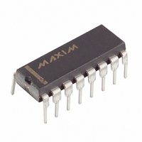
DS1640 Maxim Integrated Products, DS1640 Datasheet - Page 2

DS1640
Manufacturer Part Number
DS1640
Description
IC POWER FET PC 16-DIP
Manufacturer
Maxim Integrated Products
Type
General Purposer
Datasheet
1.DS1640S.pdf
(4 pages)
Specifications of DS1640
Number Of Outputs
4
Internal Switch(s)
Yes
Current Limit
300mA
Voltage - Input
3 ~ 5.5 V
Operating Temperature
0°C ~ 70°C
Mounting Type
Through Hole
Package / Case
16-DIP (0.300", 7.62mm)
Lead Free Status / RoHS Status
Contains lead / RoHS non-compliant
Rds (on)
-
Available stocks
Company
Part Number
Manufacturer
Quantity
Price
Company:
Part Number:
DS1640S
Manufacturer:
DALLAS
Quantity:
49
Company:
Part Number:
DS1640S
Manufacturer:
SOP-16
Quantity:
5 510
Part Number:
DS1640S
Manufacturer:
DALLAS
Quantity:
20 000
Part Number:
DS1640S+
Manufacturer:
MAXIM/美信
Quantity:
20 000
Company:
Part Number:
DS1640S+T&R
Manufacturer:
MA/COM
Quantity:
240
DS1640/DS1640C
OPERATION
With +3 Û +5 volts applied between the V
pin and ground, any one of four inputs can be connected or
CC
disconnected from its respective output based on the bias applied to the control gate (see Figure 1). A set
of four internal latches is controlled by the latch input. The logic levels passed to the FET gates are
controlled by the gate inputs and latch pin status. When the latch pin is logic 0, the gate input levels are
inverted and passed directly to the control gates, enabling the switches to be switched both independently
and asynchronously. With a transition from logic 0 to logic 1 on the latch pin, the input levels present on
the gate inputs are locked by the four internal latches, maintaining the corresponding FET gates at those
levels. As long as the latch input is maintained at logic 1, the FET gate levels are maintained. When the
latch input is returned to logic 0, the gate inputs again are inverted and passed to the FET control gates
without being latched. A TTL or CMOS logic 1 turns a switch completely on and TTL or CMOS logic 0
turns a switch completely off. The four switches can be operated independently or two or more can be
connected in parallel for added current carrying capability. The four switches contained within the
DS1640 are not designed to be operated in a linear manner. When V
is not applied to the DS1640 or if
CC
V
is not within nominal limits, the output levels and current carrying capability of the four switches are
CC
not guaranteed. When all four gate inputs are off (logic 0) the device enters a low V
current standby
CC
mode because the onboard charge pump is turned off. The gate and latch inputs are CMOS-compatible
throughout the entire V
range and are TTL-compatible when V
falls between 4.5 and 5.5V.
CC
CC
DS1640 BLOCK DIAGRAM Figure 1
2 of 4


