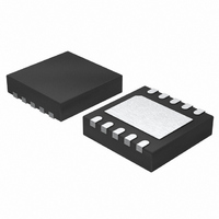
LTC3588EDD-1#PBF Linear Technology, LTC3588EDD-1#PBF Datasheet - Page 9

LTC3588EDD-1#PBF
Manufacturer Part Number
LTC3588EDD-1#PBF
Description
IC ENEGRY HARVESTING PSU 10DFN
Manufacturer
Linear Technology
Datasheet
1.LTC3588EDD-1PBF.pdf
(20 pages)
Specifications of LTC3588EDD-1#PBF
Applications
Energy Harvesting
Voltage - Supply
2.7 V ~ 20 V
Operating Temperature
-40°C ~ 85°C
Mounting Type
Surface Mount
Package / Case
10-DFN
Ic Function
Power Management IC
Supply Voltage Range
2.7V To 20V
Operating Temperature Range
-40°C To +85°C
Digital Ic Case Style
DFN
No. Of Pins
10
Msl
MSL 1 - Unlimited
Rohs Compliant
Yes
Lead Free Status / RoHS Status
Lead free / RoHS Compliant
Current - Supply
-
Available stocks
Company
Part Number
Manufacturer
Quantity
Price
OPERATION
UVLO falling threshold before the output voltage reaches
regulation, the buck converter will shut off and will not
be turned on until the input voltage again rises above the
UVLO rising threshold. During this time the output voltage
will be loaded by less than 100nA. When the buck brings
the output voltage into regulation the converter enters a
low quiescent current sleep state that monitors the output
voltage with a sleep comparator. During this operating mode
load current is provided by the buck output capacitor. When
the output voltage falls below the regulation point the buck
regulator wakes up and the cycle repeats. This hysteretic
method of providing a regulated output reduces losses
associated with FET switching and maintains an output
at light loads. The buck delivers a minimum of 100mA of
average load current when it is switching.
When the sleep comparator signals that the output has
reached the sleep threshold the buck converter may be
in the middle of a cycle with current still fl owing through
the inductor. Normally both synchronous switches would
turn off and the current in the inductor would freewheel
to zero through the NMOS body diode. The LTC3588-1
keeps the NMOS switch on during this time to prevent the
conduction loss that would occur in the diode if the NMOS
were off. If the PMOS is on when the sleep comparator
trips the NMOS will turn on immediately in order to ramp
down the current. If the NMOS is on it will be kept on until
the current reaches zero.
Though the quiescent current when the buck is switching
is much greater than the sleep quiescent current, it is still
a small percentage of the average inductor current which
results in high effi ciency over most load conditions. The
buck operates only when suffi cient energy has been ac-
cumulated in the input capacitor and the length of time the
converter needs to transfer energy to the output is much
less than the time it takes to accumulate energy. Thus, the
buck operating quiescent current is averaged over a long
period of time so that the total average quiescent current
is low. This feature accommodates sources that harvest
small amounts of ambient energy.
Four selectable voltages are available by tying the output
select bits, D0 and D1, to GND or V
the four D0/D1 codes and their corresponding output
voltages.
IN2
. Table 1 shows
Table 1. Output Voltage Selection
The internal feedback network draws a small amount of
current from V
Power Good Comparator
A power good comparator produces a logic high referenced
to V
reaches the sleep threshold of the programmed V
signaling that the output is in regulation. The PGOOD pin
will remain high until V
regulation voltage. Several sleep cycles may occur during
this time. Additionally, if PGOOD is high and V
the UVLO falling threshold, PGOOD will remain high until
V
allows output energy to be used even if the input is lost.
Figure 2 shows the behavior for V
At t = 75s V
by the quiescent current of the LTC3588-1 and through
servicing V
current. V
until V
The PGOOD pin is designed to drive a microprocessor or
other chip I/O and is not intended to drive higher current
loads such as an LED.
OUT
D1
0
0
1
1
OUT
Figure 2. PGOOD Operation During Transition to UVLO
falls to 92% of the desired regulation point. This
OUT
on the PGOOD pin the fi rst time the converter
IN
decreases to 92% of the desired regulation point.
IN
D0
OUT
crosses UVLO falling but PGOOD remains high
6
5
4
3
2
1
0
0
1
0
1
0
becomes high impedance and is discharged
OUT
which is discharged by its own leakage
as listed in Table 1.
V
1.8V
2.5V
3.3V
3.6V
OUT
100
V
IN
OUT
TIME (s)
V
IN
V
= UVLO FALLING
C
falls to 92% of the desired
OUT
VIN
PGOOD
= C
200
QUIESCENT CURRENT (I
V
OUT
VOUT
OUT
LTC3588-1
= 3.6V and no load.
= 100μF
35881 F02
44nA
62nA
81nA
89nA
300
IN
falls below
VOUT
35881fa
OUT
9
)
,


