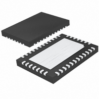
LTC3576EUFE#PBF Linear Technology, LTC3576EUFE#PBF Datasheet - Page 40

LTC3576EUFE#PBF
Manufacturer Part Number
LTC3576EUFE#PBF
Description
IC POWER MANAGER W/USB OTG 38QFN
Manufacturer
Linear Technology
Datasheet
1.LTC3576EUFEPBF.pdf
(48 pages)
Specifications of LTC3576EUFE#PBF
Applications
Handheld/Mobile Devices
Voltage - Supply
4.35 V ~ 5.5 V
Operating Temperature
-40°C ~ 85°C
Mounting Type
Surface Mount
Package / Case
38-QFN
Lead Free Status / RoHS Status
Lead free / RoHS Compliant
Current - Supply
-
Available stocks
Company
Part Number
Manufacturer
Quantity
Price
LTC3576/LTC3576-1
APPLICATIONS INFORMATION
down on-the-go A device and a powered down standard
host. A suitable pulse can be generated because of the
disparity in the bypass capacitances of an on-the-go A
device and a standard host even if there is somewhat
more than 6.5μF capacitance connected to the V
of the LTC3576/LTC3576-1.
Board Layout Considerations
The Exposed Pad on the backside of the LTC3576/
LTC3576-1 package must be securely soldered to the PC
board ground. This is the primary ground pin in the pack-
age, and it serves as the return path for both the control
circuitry and the N-channel MOSFET switches.
Furthermore, due to its high frequency switching circuitry,
it is imperative that the input capacitor, inductor, and
output capacitor be as close to the LTC3576/LTC3576-1
as possible and that there be an unbroken ground plane
under the LTC3576/LTC3576-1 and all of their external
40
TRANSCEIVER
ON-THE-GO
LTC3576-1
B DEVICE
LTC3576/
ENOTG
TRANSCEIVER
ON-THE-GO
LTC3576-1
LTC3576/
A DEVICE
ENOTG
Figure 11. LTC3576/LTC3576-1 as the A Device
Figure 12. LTC3576/LTC3576-1 as the B Device
OVSENS
OVGATE
V
BUS
OVSENS
OVGATE
V
BUS
C
<6.5μF
WITHOUT OVP
B
BUS
C
<6.5μF
WITHOUT OVP
A
pin
(OPTIONAL)
(OPTIONAL)
>96μF FOR STANDARD HOST
OVP
OVP
<6.5μF FOR OTG DEVICES
D
D
D
D
–
+
–
+
high frequency components. High frequency currents,
such as the V
their way on the ground plane along a mirror path directly
beneath the incident path on the top of the board. If there
are slits or cuts in the ground plane due to other traces
on that layer, the current will be forced to go around the
slits. If high frequency currents are not allowed to fl ow
back through their natural least-area path, excessive
voltage will build up and radiated emissions will occur
(see Figure 13). There should be a group of vias directly
under the grounded backside leading directly down to an
internal ground plane. To minimize parasitic inductance,
the ground plane should be as close as possible to the
top plane of the PC board (layer 2).
The IDGATE pin for the external ideal diode controller has
extremely limited drive current. Care must be taken to
minimize leakage to adjacent PC board traces. 100nA of
leakage from this pin will introduce an additional offset to
C
<6.5μF
B
C
A
BUS
, V
TRANSCEIVER
ON-THE-GO
ON-THE-GO
MANAGER
B DEVICE
IN1
POWER
, V
STANDARD OR
TRANSCEIVER
USB HOST OR
ON-THE-GO
ON-THE-GO
STANDARD
MANAGER
IN2
A DEVICE
POWER
3576 F11
and V
3576 F12
IN3
currents tend to fi nd
3576fb


