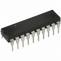
FAN7311N Fairchild Semiconductor, FAN7311N Datasheet

FAN7311N
Specifications of FAN7311N
Related parts for FAN7311N
FAN7311N Summary of contents
Page 1
... Package (1) FAN7383M 14-SOP (1) FAN7383MX Note: 1. These devices passed wave soldering test by JESD22A-111. © 2006 Fairchild Semiconductor Corporation FAN7383 Rev. 1.0.3 Description The FAN7383 is a half-bridge gate-drive IC with shutdown functions for driving MOSFETs and IGBTs that operate up to +600V. Swing to -9.8V for Fairchild’ ...
Page 2
... Typical Application Circuit V DD PWM PWM IC Shutdown Control R DT Figure 1. Application Circuit for Half-Bridge Switching Power Supply PHA IN PHB SD SD FAN7383 DC Motor Controller DT Figure 2. Application Circuit for Full-Bridge DC Motor Driver © 2006 Fairchild Semiconductor Corporation FAN7383 Rev. 1.0 BOOT BOOT HO1 HO2 ...
Page 3
... Internal Block Diagram SCHMITT 1 IN TRIGGER INPUT 2 SD SHOOT THOUGH PREVENTION DT 3 DEAD-TIME { DTMIN=330nsec } © 2006 Fairchild Semiconductor Corporation FAN7383 Rev. 1.0.3 NOISE CANCELLER HS(ON/OFF) UVLO LS(ON/OFF) Figure 3. Functional Block Diagram of FAN7383 UVLO 13 HO1 R 12 HO2 LO1 DELAY 6 LO2 7 GND FAN7383 Rev:01 ...
Page 4
... Pin Configuration Pin Definitions Pin # Name LO1 6 LO2 7 GND 8 N.C. 9 N. HO2 13 HO1 © 2006 Fairchild Semiconductor Corporation FAN7383 Rev. 1.0 HO1 HO2 LO1 LO2 GND FAN7383 Rev:00 Figure 4. Pin Configuration (Top View) Description Logic Input for Gate Driver Logic Input for Shutdown (Active Low) ...
Page 5
... High-side floating supply offset voltage S V Low-side supply voltage DD V High-side (HO) output voltage HO V Low-side (LO) output voltage LO V Logic input voltage (IN Ambient temperature A © 2006 Fairchild Semiconductor Corporation FAN7383 Rev. 1.0.3 = 25°C unless otherwise specified. A Parameter Parameter Condition 5 Min. Max. Unit V - ...
Page 6
... Logic "0" input bias current IN- SD+ Shutdown "1" input voltage SD- Shutdown "0" input voltage R Input pull-down resistance PD Note: 5.This parameter guaranteed by design. © 2006 Fairchild Semiconductor Corporation FAN7383 Rev. 1.0.3 = GND 25°C, unless otherwise specified. The V A parameters are referenced Condition V = ...
Page 7
... Turn-off fall time F (5) t Shutdown propagation delay SD DT1, Dead-time LO OFF and HO DT2 OFF DMT Dead-time matching Note: 5.These parameters guaranteed by design. © 2006 Fairchild Semiconductor Corporation FAN7383 Rev. 1.0.3 =1000pF GND, and T = 25°C, unless otherwise specified Conditions V =0V S (5) V =0V or 600V ...
Page 8
... Figure 7. V Quiescent Current vs. Temperature DD 1600 1400 1200 1000 800 600 400 -40 - Temperature [°C] Figure 9. V Operating Current vs. Temperature DD © 2006 Fairchild Semiconductor Corporation FAN7383 Rev. 1.0.3 11.6 11.4 11.2 11.0 10.8 10.6 10.4 10.2 10.0 -40 - 100 120 Figure 6. V 100 ...
Page 9
... Figure 13. Logic Input Low Voltage vs. Temperature 3.0 2.5 2.0 1.5 1.0 0.5 0.0 -40 - Temperature [°C] Figure 15. SD Negative Threshold vs. Temperature © 2006 Fairchild Semiconductor Corporation FAN7383 Rev. 1.0.3 (Continued) 3.0 2.5 2.0 1.5 1.0 0.5 0.0 - 100 120 Figure 12. Logic Input High Voltage vs. Temperature 3 ...
Page 10
... Figure 19. Turn-off Falling Time vs. Temperature 2.4 2.2 2.0 1.8 1.6 1.4 1.2 -40 - Temperature [°C] Figure 21. Dead Time (R =200kΩ) vs. Temperature DT © 2006 Fairchild Semiconductor Corporation FAN7383 Rev. 1.0.3 (Continued) 700 600 500 400 300 200 - 100 120 Figure 18. Turn-on Delay Time vs. Temperature 400 360 ...
Page 11
... Typical Characteristics -6 -8 -10 -12 -14 -40 - Temperature [°C] Figure 23. Allowable Negative V Propagation to High Side vs. Temperature © 2006 Fairchild Semiconductor Corporation FAN7383 Rev. 1.0.3 (Continued 100 120 Voltage for Signal S 11 www.fairchildsemi.com ...
Page 12
... Switching Time Definitions +15V SD LO1 HO1, 2 LO1 DT1 DT2 IN 50% t OFF 90% LO1, 2 HO1, 2 © 2006 Fairchild Semiconductor Corporation FAN7383 Rev. 1.0.3 FAN7383 10μF 100nF HO1 2 DT HO2 LO1 NC LO2 NC 6 1nF NC GND 7 FAN7383 Rev:00 Figure 24. Switching Time Test Circuit Shutdown Figure 25. Input / Output Waveforms ...
Page 13
... 90% LO © 2006 Fairchild Semiconductor Corporation FAN7383 Rev. 1.0.3 50 Figure 27. Shutdown Waveform Definition 10% DT1 MDT= DT1-DT2 Figure 28. Dead-Time Waveform Definition 13 90% FAN7383 Rev:00 90% DT2 10% FAN7383 Rev:00 www.fairchildsemi.com ...
Page 14
... The UVLO circuitry monitors the supply voltage (V ) and bootstrap capacitor voltage independently. BS © 2006 Fairchild Semiconductor Corporation FAN7383 Rev. 1.0.3 3. Layout Consideration For optimum performance of high- and low-side gate drivers, cannot be achieved without taking due considerations must be taken during printed circuit board (PCB) layout. ...
Page 15
... Package Dimensions 14-SOP Dimensions are in millimeters unless otherwise noted 0.60 ±0.20 ±0.008 0.024 © 2006 Fairchild Semiconductor Corporation FAN7383 Rev. 1.0.3 #14 #8 ±0.30 6.00 ±0.012 0.236 3.95 ±0.20 ±0.008 0.156 5.72 0.225 Figure 29. 14-Lead Small Outline Package (SOP) 15 0.05 MIN 0.002 1.55 ± ...
Page 16
... TRADEMARKS The following are registered and unregistered trademarks Fairchild Semiconductor owns or is authorized to use and is not intended exhaustive list of all such trademarks. ® ACEx Across the board. Around the world. ActiveArray Bottomless Build it Now CoolFET CROSSVOLT CTL™ Current Transfer Logic™ ...


