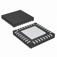
MAX1517ETJ+ Maxim Integrated Products, MAX1517ETJ+ Datasheet - Page 2

MAX1517ETJ+
Manufacturer Part Number
MAX1517ETJ+
Description
IC DC/DC CONV TFT-LCD 32-TQFN
Manufacturer
Maxim Integrated Products
Datasheet
1.MAX1517ETJ.pdf
(26 pages)
Specifications of MAX1517ETJ+
Applications
LCD Display, Automotive
Voltage - Supply
2.6 V ~ 5.5 V
Operating Temperature
-40°C ~ 85°C
Mounting Type
Surface Mount
Package / Case
32-TQFN Exposed Pad
Lead Free Status / RoHS Status
Lead free / RoHS Compliant
Current - Supply
-
Lead Free Status / Rohs Status
Lead free / RoHS Compliant
ABSOLUTE MAXIMUM RATINGS
IN, CTL to AGND ......................................................-0.3V to +6V
COMP, FB, FBP, FBN, DEL, REF to AGND ....-0.3V to (V
PGND, BGND to AGND ......................................................±0.3V
LX to PGND ............................................................-0.3V to +14V
SUP to AGND .........................................................-0.3V to +14V
DRVP, SRC to AGND..............................................-0.3V to +30V
POS_, NEG_, OUT_ to AGND ...................-0.3V to (V
POS1 to NEG1, POS2 to NEG2, POS3 to NEG3,
DRVN to AGND ...................................(V
TFT-LCD DC-DC Converters with
Operational Amplifiers
Stresses beyond those listed under “Absolute Maximum Ratings” may cause permanent damage to the device. These are stress ratings only, and functional
operation of the device at these or any other conditions beyond those indicated in the operational sections of the specifications is not implied. Exposure to
absolute maximum rating conditions for extended periods may affect device reliability.
ELECTRICAL CHARACTERISTICS
(V
wise noted.)
2
IN Supply Range
IN Undervoltage-Lockout
Threshold
IN Quiescent Current
Duration to Trigger Fault
Condition
REF Output Voltage
Thermal Shutdown
MAIN STEP-UP REGULATOR
Output Voltage Range
Operating Frequency
Oscillator Maximum Duty Cycle
FB Regulation Voltage
FB Fault Trip Level
FB Load Regulation
FB Line Regulation
FB Input Bias Current
FB Transconductance
FB Voltage Gain
IN
POS4 to NEG4, POS5 to NEG5 ...............................-6V to +6V
_______________________________________________________________________________________
= 3V, V
PARAMETER
SUP
= 8V, PGND = AGND = BGND = 0, I
SYMBOL
V
V
IN
f
UVLO
V
V
MAIN
OSC
I
IN
FB
IN
- 30V) to (V
V
V
LX not switching
V
LX switching
-2µA < I
Temperature rising
Hysteresis
No load
V
0 < I
V
V
FB to COMP
IN
FB
FB
FB
IN
FB
I
SUP
COMP
REF
IN
IN
rising, typical hysteresis = 150mV
= 2.6V to 5.5V
= V
= 1.1V, V
falling
= 1.4V
MAIN
+ 0.3V)
+ 0.3V)
+ 0.3V)
= 25µA, T
FBP
REF
= 5µA
< full load, transient only
= 1.4V, V
< 50µA, V
FBP
CONDITIONS
A
= 1.4V, V
= 0°C to +85°C. Typical values are at T
COM, DRN to AGND ................................-0.3V to (V
DRN to COM............................................................-30V to +30V
OUT_ Maximum Continuous Output Current....................±75mA
LX Switch Maximum Continuous RMS Output Current .........1.6A
Continuous Power Dissipation (T
Operating Temperature Range .........................-40°C to +100°C
Junction Temperature ......................................................+150°C
Storage Temperature Range .............................-65°C to +150°C
Lead Temperature (soldering, 10s) .................................+300°C
FBN
T
T
32-Pin Thin QFN (derate 21.2mW/°C above +70°C) ..1702mW
IN
A
A
= +25 C to +85 C
= 0 C to +85 C
= 2.6V to 5.5V
= 0,
FBN
= 0,
1.231
1.221
1.218
1020
MIN
0.96
V
-40
2.6
2.3
84
75
IN
A
= +70°C)
+0.04
1.250
1.233
1.233
+160
1200
TYP
1.00
-1.6
150
600
2.5
0.6
55
15
87
6
A
= +25°C, unless other-
1.269
1.245
1.247
MAX
1380
1.04
+40
280
5.5
2.7
0.8
0.15
11
13
90
SRC
UNITS
+ 0.3V)
%/ V
kHz
mA
V/ V
ms
nA
µS
%
%
V
V
V
V
V
V
C


