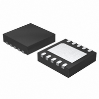
LT3585EDDB-2#TRPBF Linear Technology, LT3585EDDB-2#TRPBF Datasheet - Page 10

LT3585EDDB-2#TRPBF
Manufacturer Part Number
LT3585EDDB-2#TRPBF
Description
IC CHARGER PHOTOFLASH 10-DFN
Manufacturer
Linear Technology
Datasheet
1.LT3585EDDB-2TRPBF.pdf
(20 pages)
Specifications of LT3585EDDB-2#TRPBF
Applications
Photoflash Capacitor Charger, Xenon
Current - Supply
5mA
Voltage - Supply
1.5 V ~ 16 V
Operating Temperature
-40°C ~ 85°C
Mounting Type
Surface Mount
Package / Case
10-DFN
Lead Free Status / RoHS Status
Lead free / RoHS Compliant
Available stocks
Company
Part Number
Manufacturer
Quantity
Price
OPERATIO
LT3585-0/LT3585-1
LT3585-2/LT3585-3
The LT3585 series of parts operate on the edge of dis-
continuous conduction mode. When CHRG/IADJ is driven
higher than 1.1V, the master latch is set. This enables the
part to deliver power to the photofl ash capacitor. When
the power switch, Q1, is turned on, current builds up in
the primary of the transformer. When the desired current
level is reached, the output of comparator A1 goes high,
resetting the switch latch that controls the state of Q1, and
the output of the DCM comparator goes low. Q1 now turns
off and the fl yback waveform on the SW node quickly rises
to a level proportional to V
through high voltage diode(s), D1, and into the photofl ash
capacitor. When the secondary current decays to zero,
the voltage on the SW node collapses. When this voltage
reaches 130mV higher than V
high. This sets the switch latch and the power switch, Q1,
turns back on. This cycle repeats until the target V
is reached. When the target V
latch resets and the DONE pin goes low.
The input current of an LT3585 series circuit can be
reduced by changing the voltage of the CHRG/IADJ pin.
When this pin is between 1.1V and 1.4V, a time delay is
10
V
V
I
I
PRI
SW
PRI
SW
Figure 2. Normal and Reduced Input Current Waveforms
U
Reduced Input Current
Normal Operation
CHRG/IADJ Three Stated
(~5.2µs at V
CHRG/IADJ ≥ 1.6V
Extra Delay Added
OUT
TIME
TIME
TIME
TIME
. The secondary current fl ows
BAT
OUT
BAT
= 4.2V)
, the output of A3 goes
is reached, the master
3585 F02
OUT
level
added between when A3 goes high and the switch latch
is set, see Figure 2. If the part is enabled, and the CHRG/
IADJ pin is fl oated, internal circuitry drives the voltage on
the pin to 1.28V. This allows a single I/O port pin, which
can be three-stated, to enable or disable the part as well
as place the part into the input current reduction mode.
This feature effectively reduces the average input current
into the fl yback transformer. The magnitude of the delay
decreases with increasing V
average input current to remain relatively fl at with changes
in V
no delay is added. The CHRG/IADJ pin functionality is
shown in Figure 3.
Both V
one of these pins goes below its UVLO voltage, the DONE
pin goes low. With an insuffi cient bypass capacitor on V
or V
terminate the charge. The applications circuits in the data
sheet suggest values adequate for most applications.
The LT3585 series also includes an integrated IGBT driver.
There are two output pins, IGBTPU and IGBTPD. The
IGBTPU pin is used to pull the gate of the IGBT up. This
should be done quickly to guarantee proper Xenon lamp
ignition. Tie this pin directly to the gate of the IGBT. The
IGBTPD pin is pinned out separately to allow for greater
fl exibility in choosing a series resistor between the pin and
the gate of the IGBT. This resistor can be used to slow
down the turn off of the IGBT.
CHRG/IADJ
BAT
100V/DIV
IN
2V/DIV
2V/DIV
, the ripple on the pin is likely to activate UVLO and
BAT
DONE
V
. When CHRG/IADJ is brought higher than 1.6V,
<0.3V
*MUST TAKE CHRG/IADJ PIN ABOVE 1.1V, THEN FLOAT
OUT
and V
LT3585-1
V
C
BAT
OUT
STATE*
THREE
= 3.6V
= 50µF
IN
have undervoltage lockout (UVLO). When
Figure 3. Basic Operation
CHRG/IADJ PIN STATE
3V
1sec/DIV
<0.3V
BAT
. This causes the reduced
3V
<0.3V
3585 F03
3585f
BAT


