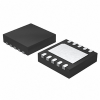
LT3585EDDB-3#TRPBF Linear Technology, LT3585EDDB-3#TRPBF Datasheet - Page 8

LT3585EDDB-3#TRPBF
Manufacturer Part Number
LT3585EDDB-3#TRPBF
Description
IC CHARGER PHOTOFLASH 10-DFN
Manufacturer
Linear Technology
Datasheet
1.LT3585EDDB-2TRPBF.pdf
(20 pages)
Specifications of LT3585EDDB-3#TRPBF
Applications
Photoflash Capacitor Charger, Xenon
Current - Supply
5mA
Voltage - Supply
1.5 V ~ 16 V
Operating Temperature
-40°C ~ 85°C
Mounting Type
Surface Mount
Package / Case
10-DFN
Lead Free Status / RoHS Status
Lead free / RoHS Compliant
Available stocks
Company
Part Number
Manufacturer
Quantity
Price
PI FU CTIO S
LT3585-0/LT3585-1
LT3585-2/LT3585-3
IGBTIN (Pin 1): Logic Input for the IGBT Driver. When this
pin is driven higher than 1.5V, the output goes high. When
the pin is below 0.5V, the output will go low.
IGBTPWR (Pin 2): Supply Pin for the IGBT Driver. Must be
locally bypassed with a good quality ceramic capacitor. The
minimum operating voltage for the IGBT driver is 2.5V.
GND (Pin 3): Ground. Tie directly to local ground plane.
V
with a good quality ceramic capacitor. The minimum
operating voltage for V
V
with a good quality ceramic capacitor. The minimum
operating voltage for V
DONE (Pin 6): Open NPN Collector Indication Pin. When
target output voltage is reached, NPN turns on. This pin
needs a proper pull-up resistor or current source.
CHRG/IADJ (Pin 7): Charge and Input Current Adjust Pin.
A low (<0.3V) to high (>1.1V) transition on this pin puts
the part into power delivery mode. Once the target output
voltage is reached, the part will stop charging the output.
Toggle this pin to start charging again. Ground to shut
down. To enter into the input current reduction mode, the
8
IN
BAT
U
(Pin 4): Input Supply Pin. Must be locally bypassed
(Pin 5): Battery Supply Pin. Must be locally bypassed
U
U
IN
BAT
is 2.5V.
is 1.5V.
voltage on this pin should be driven high ( >1.1V ) and
then fl oated. (For more information refer to the Operation
section of this data sheet.) To enter normal mode, the
voltage should be driven higher than 1.6V.
SW (Pin 8): Switch Pin. This is the collector of the internal
NPN Power switch. Minimize the metal trace area connected
to this pin to minimize EMI. Tie one side of the primary
of the transformer to this pin. The target output voltage
is set by the turns ratio of the transformer.
Choose turns ratio N by the following equation:
where V
IGBTPD (Pin 9): Pull-down Output for IGBT Gate. Connect
this pin to the IGBT Gate. Add a series resistor to increase
the turn-off time to protect the IGBT.
IGBTPU (Pin 10): Pull-up Output for IGBT Gate. Connect
this pin to the gate of the IGBT.
Exposed Pad (Pin 11): Ground. Tie directly to local ground
plane.
N
=
V
OUT
OUT
31 5 .
is the desired output voltage.
+ 2
3585f


