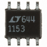
LTC1153CS8 Linear Technology, LTC1153CS8 Datasheet - Page 5

LTC1153CS8
Manufacturer Part Number
LTC1153CS8
Description
IC ELECTR CIRCUIT BREAKER 8-SOIC
Manufacturer
Linear Technology
Datasheet
1.LTC1153CS8PBF.pdf
(16 pages)
Specifications of LTC1153CS8
Applications
Overvoltage Protection, Circuit Breaker
Current - Supply
180µA
Voltage - Supply
4.5 V ~ 18 V
Operating Temperature
0°C ~ 70°C
Mounting Type
Surface Mount
Package / Case
8-SOIC (3.9mm Width)
Lead Free Status / RoHS Status
Contains lead / RoHS non-compliant
Available stocks
Company
Part Number
Manufacturer
Quantity
Price
Company:
Part Number:
LTC1153CS8
Manufacturer:
LT
Quantity:
10 000
Part Number:
LTC1153CS8
Manufacturer:
LINEAR/凌特
Quantity:
20 000
Part Number:
LTC1153CS8#TRPBF
Manufacturer:
LINEAR/凌特
Quantity:
20 000
PI FU CTIO S
TYPICAL PERFOR
Input and Shutdown Pins
The LTC1153 input pin is active high and activates all of the
protection and charge pump circuitry when switched ON.
The shutdown pin is designed to break the circuit if a
secondary fault condition (over temperature, etc.) is de-
tected. The LTC1153 logic and shutdown inputs are high
impedance CMOS gates with ESD protection diodes to
ground and supply and therefore should not be forced
beyond the power supply rails. The shutdown pin should
be connected to ground when not in use.
Timing Capacitor Pin (Auto-Reset Timer)
The small capacitor charging current (4.2 A) produces
large delays with relatively small valued capacitors, but
care must be taken to ensure that this current is not
shunted to ground through a leaky capacitor or printed
circuit board trace. The timing capacitor voltage is sensed
by a high impedance CMOS comparator input with ESD
clamp diodes to ground and supply and therefore should
not be forced beyond the power supply rails. This pin can
be grounded if the auto-reset function is not used.
MOSFET Gate Drive Pin
The MOSFET gate drive pin is either driven to ground when
the switch is turned OFF or driven above the supply rail
when the switch is turned ON. This pin is a relatively high
1.6
1.O
2.4
2.2
2.0
1.8
1.4
1.2
0.8
0.6
0.4
U
–50
Shutdown Threshold Voltage
–25
U
0
TEMPERATURE (°C)
25
V
V
U
50
S
S
= 5V
= 18V
75
W
LTC1153 • TPC13
100
A
U
125
CE
C
HARA TERISTICS
0.1
10
1
–50
Auto-Reset Time*
*SECONDS OF DELAY
PER F C
–25
C
T
0
TEMPERATURE (°C)
V
V
V
S
S
S
= 18V
= 12V
25
= 5V
impedance when driven above the rail (the equivalent of a
few hundred k ). Care should be taken to minimize any
loading of this pin by parasitic resistance to ground or
supply.
Supply Pin
The supply pin of the LTC1153 serves two vital purposes.
The first is obvious: it powers the input, gate drive, regu-
lation and protection circuitry. The second purpose is less
obvious: it provides a Kelvin connection to the top of the
drain sense resistor for the internal 100mV reference.
The LTC1153 is designed to be continuously powered so
that the gate of the MOSFET is actively driven at all times.
If it is necessary to remove power from the supply pin and
then re-apply it, the input pin (or enable pin) should be
cycled a few milliseconds after the power is re-applied to
reset the input latch and protection circuitry. Also, the
input and enable pins should be isolated with 10k resistors
to limit the current flowing through the ESD protection
diodes to the supply pin.
The supply pin of the LTC1153 should never be forced
below ground as this may result in permanent damage to
the device. A 300 resistor should be inserted in series
with the ground pin if negative supply voltage transients
are anticipated.
50
75
LTC1153 • TPC14
100
125
1000
100
0.1
10
1
0
MOSFET Gate Drive Current
T
A
= 25°C
GATE VOLTAGE ABOVE SUPPLY (V)
V
S
4
= 5V
V
8
S
= 12V
LTC1153
12
V
S
= 18V
LTC1153 • TPC15
16
5
20


