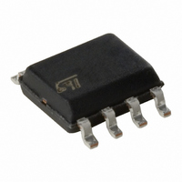
L6615D STMicroelectronics, L6615D Datasheet

L6615D
Specifications of L6615D
Available stocks
Related parts for L6615D
L6615D Summary of contents
Page 1
... CGA CGA L6615 L6615 L6615 L6615 BCD TECHNOLOGY DIP8 SO8 ORDERING NUMBERS: L6615N L6615D L6615DTR(T & Reel) +OUT +OUT +OUT LOAD LOAD LOAD GND GND GND ( * ) OR-ing FET can ( * ) OR-ing FET can be used to reduce be used to reduce power dissipation power dissipation 1/20 ...
Page 2
L6615 DESCRIPTION (continued) Load sharing is a technique used in all the systems in which the load requires low voltage, high current and/or redundancy; for this reason a modular power system is necessary in which two or more power sup- ...
Page 3
ABSOLUTE MAXIMUM RATINGS Symbol Pin CS ADJ CGA V 5 COMP ( ...
Page 4
L6615 ELECTRICAL CHARACTERISTCS (Tj = -40 to 85°C, Vcc=12V, V ADJ SENSE L SENSE G1 G2 Symbol Parameter Vcc V Operating range cc I Quiescent current cc V Turn-on voltage CC, ...
Page 5
ELECTRICAL CHARACTERISTCS (continued) (Tj = -40 to 85°C, Vcc=12V, V ADJ SENSE L SENSE G1 G2 Symbol Parameter I Source current OH I Sink current OL V Low voltage COMP(L) V ...
Page 6
L6615 Figure 1. Turn-on and turn-off voltage [V] CC(ON) CC(OFF) 3 2.6 2.2 - Figure 2. Supply current vs. supply voltage I [ mA] CC 100 10 1 0.1 0.01 ...
Page 7
Figure 7. Share bus input impedance Figure 8. ADJ maximum current I [mA] AD J[MAX ...
Page 8
L6615 APPLICATION INFORMATION Index 1. Introduction 2. Current sense section 3. Share drive section, error amplifier and adjust amplifier 4. Designing with L6615 5. Current sense methods 6. Application ideas 7. Low voltage buses 8. Offset Trimming 1 INTRODUCTION Power ...
Page 9
CURRENT SENSE SECTION A sense resistor is typically used to generate the voltage drop, proportional to the load current, measured by the CSA (Current Sense Amplifier), whose input pins (pins #2 and #3) are connected across of R through ...
Page 10
L6615 3 SHARE DRIVE SECTION, ERROR AMPLIFIER AND ADJUST AMPLIFIER The gain between the output of CSA (CGA pin) and output of SDA (SH pin (typ.) so, for the master power supply the voltage ...
Page 11
L6615 V – V represents an upper limit but the designer should select the full scale share bus voltage SH(MAX) keeping in mind that every Volt on the ...
Page 12
L6615 Figure 12. ADJ network E/A E REF REF To set the R value it is necessary to know the tolerance required of the power supply output voltage ADJ (V ± the maximum difference between master ...
Page 13
The last point is the design of the compensation network Z ground. Besides the power supply feedback loop, the current sharing system introduces another, outer loop. To avoid interaction between them it is important to design the bandwidth of the ...
Page 14
L6615 Figure 13. Current sense methods. L6615 L6615 CS+ CS+ CS- CS SNS SNS OUT OUT POWER POWER SUPPLY SUPPLY D D ...
Page 15
Figure 15. Distributed power system for +48V bus +48V +48V (*) feedback AC AC Mains Mains +48V GND +12V DPS1 (*) the center of the output feedback divider is usually connected to a voltage compatible with L6615 AMR In this ...
Page 16
L6615 Consider, for example an application with V at CS+: is lower than 1.6V so the internal comparator triggers on the LSA structure and the pin CS- sources the current I (see paragraph "2. CURRENT SENSE SECTION"). The IC works ...
Page 17
Figure 16. Offset Trimming Because of the tolerance of the output voltage not possible to delete completely the effect of the offset on CGA pin on all the allowed output voltage range: if the trimming operation is performed ...
Page 18
L6615 mm DIM. MIN. TYP. MAX. A 3.32 a1 0.51 0.020 B 1.15 1.65 0.045 b 0.356 0.55 0.014 b1 0.204 0.304 0.008 D 10.92 E 7.95 9.75 0.313 e 2.54 e3 7.62 e4 7.62 F 6.6 I 5.08 L ...
Page 19
DIM. MIN. TYP. MAX. A 1.75 a1 0.1 0.25 0.004 a2 1.65 a3 0.65 0.85 0.026 b 0.35 0.48 0.014 b1 0.19 0.25 0.007 C 0.25 0.5 0.010 c1 45 (typ.) D (1) 4.8 5.0 0.189 E 5.8 6.2 ...
Page 20
... No license is granted by implication or otherwise under any patent or patent rights of STMicroelectronics. Specifications mentioned in this publication are subject to change without notice. This publication supersedes and replaces all information previously supplied. STMicroelectronics products are not authorized for use as critical components in life support devices or systems without express written approval of STMicroelectronics ...


