L9951 STMicroelectronics, L9951 Datasheet - Page 7
L9951
Manufacturer Part Number
L9951
Description
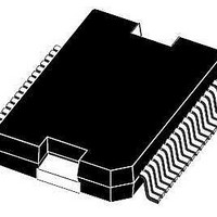
IC REAR DOOR ACT DVR POWERSO-36
Manufacturer
STMicroelectronics
Type
DC Motor Driverr
Datasheet
1.L9951XPTR.pdf
(36 pages)
Specifications of L9951
Applications
Automotive
Current - Supply
7mA
Voltage - Supply
7 V ~ 28 V
Operating Temperature
-40°C ~ 150°C
Mounting Type
Surface Mount
Package / Case
PowerSO-36 Exposed Bottom Pad
Operating Current
20mA
Operating Temperature Classification
Automotive
Motor Controller Type
DC Motor Driver
Package Type
PowerSO
Operating Supply Voltage (min)
7V
Operating Supply Voltage (max)
28V
Supply Current
20 mA
Mounting Style
SMD/SMT
Lead Free Status / RoHS Status
Lead free / RoHS Compliant
Available stocks
Company
Part Number
Manufacturer
Quantity
Price

Part Number:
L9951
Manufacturer:
ST
Quantity:
20 000
Part Number:
L9951XP
Manufacturer:
ST
Quantity:
20 000
Company:
Part Number:
L9951XPTR
Manufacturer:
st
Quantity:
6 966
Part Number:
L9951XPTR
Manufacturer:
ST
Quantity:
20 000


L9951 / L9951XP
Table 2.
15, 23, 24,
1, 18, 19,
6, 7, 14,
3, 4, 34
29, 32
Pin
36
10
11
12
13
8
9
Pin definitions and functions
CM/PWM
Symbol
OUT1
GND
CSN
VCC
CLK
DO
VS
DI
Ground .
Reference potential.
Note: For the capability of driving the full current at the outputs all pins of
GND must be externally connected.
Power supply voltage (external reverse protection required).
For EMI reason a ceramic capacitor as close as possible to GND is
recommended.
Note: for the capability of driving the full current at the outputs all pins of
VS must be externally connected.
Half-bridge output 1.
The output is built by a high side and a low side switch, which are
internally connected. The output stage of both switches is a power
DMOS transistor. Each driver has an internal reverse diode (bulk-drain-
diode: high side driver from output to VS, low side driver from GND to
output). This output is over-current and open-load protected.
Note: for the capability of driving the full current at the outputs all pins of
OUT1 must be externally connected.
Serial data input.
The input requires CMOS logic levels and receives serial data from the
microcontroller. The data is a 16bit control word and the least significant
bit (LSB, bit 0) is transferred first.
Current monitor output/PWM input.
Depending on the selected multiplexer bits (bit 9, 10, 11) of Input Data
Register this output sources an image of the instant current through the
corresponding high side driver with a ratio of 1/10.000. This pin is
bidirectional. The microcontroller can overwrite the current monitor signal
to provide a PWM input for all outputs.
Testmode:
If CSN is raised above 7.5V the device will enter the test mode. In test
mode this output can be used to measure some internal signals (see
Table
Chip select not input / Testmode .
This input is low active and requires CMOS logic levels. The serial data
transfer between L9951 and micro controller is enabled by pulling the
input CSN to low level. If an input voltage of more than 7.5V is applied to
CSN pin the L9951 will be switched into a test mode.
Serial data output .
The diagnosis data is available via the SPI and this tristate-output. The
output will remain in tristate, if the chip is not selected by the input CSN
(CSN = high).
Logic supply voltage .
For this input a ceramic capacitor as close as possible to GND is
recommended.
Serial clock input .
This input controls the internal shift register of the SPI and requires
CMOS logic levels.
Doc ID 14173 Rev 8
18).
Function
Block diagram and pin description
7/36
Related parts for L9951
Image
Part Number
Description
Manufacturer
Datasheet
Request
R

Part Number:
Description:
STMicroelectronics [RIPPLE-CARRY BINARY COUNTER/DIVIDERS]
Manufacturer:
STMicroelectronics
Datasheet:
Part Number:
Description:
STMicroelectronics [LIQUID-CRYSTAL DISPLAY DRIVERS]
Manufacturer:
STMicroelectronics
Datasheet:

Part Number:
Description:
BOARD EVAL FOR MEMS SENSORS
Manufacturer:
STMicroelectronics
Datasheet:
Part Number:
Description:
NPN TRANSISTOR POWER MODULE
Manufacturer:
STMicroelectronics
Datasheet:
Part Number:
Description:
TURBOSWITCH ULTRA-FAST HIGH VOLTAGE DIODE
Manufacturer:
STMicroelectronics
Datasheet:
Part Number:
Description:
Manufacturer:
STMicroelectronics
Datasheet:
Part Number:
Description:
DIODE / SCR MODULE
Manufacturer:
STMicroelectronics
Datasheet:
Part Number:
Description:
DIODE / SCR MODULE
Manufacturer:
STMicroelectronics
Datasheet:
Part Number:
Description:
Search -----> STE16N100
Manufacturer:
STMicroelectronics
Datasheet:
Part Number:
Description:
Search ---> STE53NA50
Manufacturer:
STMicroelectronics
Datasheet:
Part Number:
Description:
NPN Transistor Power Module
Manufacturer:
STMicroelectronics
Datasheet:
Part Number:
Description:
DIODE / SCR MODULE
Manufacturer:
STMicroelectronics
Datasheet: