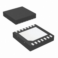
LP3905SD-30/NOPB National Semiconductor, LP3905SD-30/NOPB Datasheet - Page 7

LP3905SD-30/NOPB
Manufacturer Part Number
LP3905SD-30/NOPB
Description
IC PWR MANAGEMENT DUAL 14-LLP
Manufacturer
National Semiconductor
Datasheet
1.LP3905SDX-00NOPB.pdf
(15 pages)
Specifications of LP3905SD-30/NOPB
Applications
Handheld/Mobile Devices
Voltage - Supply
3 V ~ 5.5 V
Operating Temperature
-40°C ~ 85°C
Mounting Type
Surface Mount
Package / Case
14-LLP
For Use With
LP3905SD-30EV - BOARD EVALUATION LP3905SD-30
Lead Free Status / RoHS Status
Lead free / RoHS Compliant
Current - Supply
-
Other names
LP3905SD-30
LP3905SD-30TR
LP3905SD-30TR
Typical Application Circuit
Functional Description
POWER UP/DOWN PROCEDURE
The LP3905 Bucks and LDOs are powered UP/DOWN with
2 control pins, EN1 and EN2. In order for the enable pins to
operate, V
than V
EN1 and EN2 can be controlled fully independently.
LDOs will be turned on only after Buck1 is powered up. LDOs are powered on simultaneously.
In case EN1 and EN2 are enabled at the same time, power up of Buck2 is delayed by 50µs in order to minimize the inrush current
from the battery.
When EN1 and EN2 are disabled, the relevant output voltages are turned off.
UVLO_R
IN1
and V
(specified in electrical characteristic). Once
IN2
should be set to a voltage level higher
FIGURE 5. Typical Application Circuit For Adjustable Device
FIGURE 6. LP3905 Power UP/DOWN Timing Sequence
7
enabled, EN1 will turn on Buck1, LDO1 and LDO2. EN2 can
independently be used to enable Buck2. Figure 6 illustrates
the power UP/DOWN timing sequence of the LP3905 blocks
for V
Both linear regulators have active pulldowns when the out-
puts are disabled.
EN
≥ V
IH (min)
(enable) and V
20152904
EN
20152911
≤V
IL (max)
(disable).
www.national.com


