MAX8588ETM+T Maxim Integrated Products, MAX8588ETM+T Datasheet - Page 16
MAX8588ETM+T
Manufacturer Part Number
MAX8588ETM+T
Description
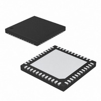
IC PMIC HI EFF LOW IQ 48-TQFN
Manufacturer
Maxim Integrated Products
Datasheet
1.MAX8588ETMT.pdf
(31 pages)
Specifications of MAX8588ETM+T
Applications
Processor
Voltage - Supply
2.6 V ~ 5.5 V
Operating Temperature
-40°C ~ 85°C
Mounting Type
Surface Mount
Package / Case
48-TQFN Exposed Pad
Lead Free Status / RoHS Status
Lead free / RoHS Compliant
Current - Supply
-
Lead Free Status / Rohs Status
Lead free / RoHS Compliant


High-Efficiency, Low-I
Dynamic Core for PDAs and Smartphones
16
PIN
EP
35
36
37
38
39
40
41
42
43
44
45
46
47
48
______________________________________________________________________________________
NAME
SRAD
RSO
CC3
ON6
ON1
PG1
FB3
LX1
PV1
SLP
DBI
MR
IN6
V6
EP
Serial Address Bit. SRAD allows the serial address to be changed in case it conflicts with another serial
device. If SRAD = GND, A1 = 0. If SRAD = IN, A1 = 1.
Open-Drain Reset Output. Deasserts when V7 exceeds 2.55V (typ rising). Has 65ms delay before release.
RSO is expected to connect to nRESET on the CPU.
Manual Reset Input. A low input at MR causes the RSO output to go low and also resets the V3 output to its
default 1.3V setting. MR impacts no other functions.
REG 3 Compensation Node. Connect a series resistor and capacitor from CC3 to GND to compensate the
regulation loop. See the Compensation and Stability section.
REG3 Feedback-Sense Input. Connect directly to the REG3 output voltage. Output voltage is set by the serial
interface.
On/Off Input for REG6. Drive high to turn on. When enabled, the REG6 output activates. ON6 has hysteresis
so an RC can be used to implement manual sequencing with respect to other inputs. It is expected that ON1,
ON2, and ON6 are connected to SYS_EN.
Also known as VCC_USIM. Linear-regulator output. This voltage is programmable through the I
0V, 1.8V, 2.5V, or 3.0V. The default voltage is 0V. REG6 is activated when ON6 is high.
Power Input to the V6 LDO. Typically connected to V1, but can also connect to IN.
REG1 Power Ground. Connect directly to a power-ground plane. Connect PG1, PG2, PG3, and GND
together at a single point as close to the IC as possible.
REG1 Switching Node. Connects to the REG1 inductor.
REG1 Power Input. Bypass to PG2 with a 4.7µF or greater low-ESR ceramic capacitor. PV1, PV2, PV3, and IN
must connect together externally.
On/Off Input for REG1. Drive high to turn on REG1. When enabled, the REG1 output soft-starts. ON1 has
hysteresis so an RC can be used to implement manual sequencing with respect to other inputs. It is
expected that ON1, ON2, and ON6 connect to SYS_EN.
Sleep Input. SLP selects which regulators ON1 and ON2 turn on. SLP = high is normal operation (ON1 and
ON2 are the enables for the V1 and V2 DC-DC converters). SLP = low is sleep operation (ON1 and ON2 are
the enables for the V1 and V2 LDOs).
Dual-Mode, Dead-Battery Input. Connect DBI to IN to set the dead-battery falling threshold to 3.15V (no
resistors needed). Connect DBI to a resistor-divider for an adjustable DBI threshold.
Exposed Metal Pad. Connect the exposed pad to ground. Connecting the exposed pad to ground does not
remove the requirement for proper ground connections to the appropriate ground pins.
Q
PMIC with
FUNCTION
Pin Description (continued)
2
C interface to
Related parts for MAX8588ETM+T
Image
Part Number
Description
Manufacturer
Datasheet
Request
R

Part Number:
Description:
High-Efficiency Low-IQ PMIC
Manufacturer:
Maxim Integrated Products
Datasheet:
Part Number:
Description:
MAX7528KCWPMaxim Integrated Products [CMOS Dual 8-Bit Buffered Multiplying DACs]
Manufacturer:
Maxim Integrated Products
Datasheet:
Part Number:
Description:
Single +5V, fully integrated, 1.25Gbps laser diode driver.
Manufacturer:
Maxim Integrated Products
Datasheet:
Part Number:
Description:
Single +5V, fully integrated, 155Mbps laser diode driver.
Manufacturer:
Maxim Integrated Products
Datasheet:
Part Number:
Description:
VRD11/VRD10, K8 Rev F 2/3/4-Phase PWM Controllers with Integrated Dual MOSFET Drivers
Manufacturer:
Maxim Integrated Products
Datasheet:
Part Number:
Description:
Highly Integrated Level 2 SMBus Battery Chargers
Manufacturer:
Maxim Integrated Products
Datasheet:
Part Number:
Description:
Current Monitor and Accumulator with Integrated Sense Resistor; ; Temperature Range: -40°C to +85°C
Manufacturer:
Maxim Integrated Products
Part Number:
Description:
TSSOP 14/A�/RS-485 Transceivers with Integrated 100O/120O Termination Resis
Manufacturer:
Maxim Integrated Products
Part Number:
Description:
TSSOP 14/A�/RS-485 Transceivers with Integrated 100O/120O Termination Resis
Manufacturer:
Maxim Integrated Products
Part Number:
Description:
QFN 16/A�/AC-DC and DC-DC Peak-Current-Mode Converters with Integrated Step
Manufacturer:
Maxim Integrated Products
Part Number:
Description:
TDFN/A/65V, 1A, 600KHZ, SYNCHRONOUS STEP-DOWN REGULATOR WITH INTEGRATED SWI
Manufacturer:
Maxim Integrated Products
Part Number:
Description:
Integrated Temperature Controller f
Manufacturer:
Maxim Integrated Products
Part Number:
Description:
SOT23-6/I�/45MHz to 650MHz, Integrated IF VCOs with Differential Output
Manufacturer:
Maxim Integrated Products
Part Number:
Description:
SOT23-6/I�/45MHz to 650MHz, Integrated IF VCOs with Differential Output
Manufacturer:
Maxim Integrated Products
Part Number:
Description:
EVALUATION KIT/2.4GHZ TO 2.5GHZ 802.11G/B RF TRANSCEIVER WITH INTEGRATED PA
Manufacturer:
Maxim Integrated Products