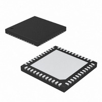
MAX1586AETM+ Maxim Integrated Products, MAX1586AETM+ Datasheet - Page 25

MAX1586AETM+
Manufacturer Part Number
MAX1586AETM+
Description
IC POWER MANAGEMENT 48-TQFN
Manufacturer
Maxim Integrated Products
Datasheet
1.MAX1587CETLT.pdf
(30 pages)
Specifications of MAX1586AETM+
Applications
Handheld/Mobile Devices
Voltage - Supply
2.6 V ~ 5.5 V
Operating Temperature
-40°C ~ 85°C
Mounting Type
Surface Mount
Package / Case
48-TQFN Exposed Pad
Dc
06+
Lead Free Status / RoHS Status
Lead free / RoHS Compliant
Current - Supply
-
Lead Free Status / Rohs Status
Lead free / RoHS Compliant
source and reduces switching noise in the controller.
The impedance of the input capacitor at the switching
frequency should be less than that of the input source
so high-frequency switching currents do not pass
through the input source.
The output capacitor keeps output ripple small and
ensures control-loop stability. The output capacitor
must also have low impedance at the switching fre-
quency. Ceramic, polymer, and tantalum capacitors
are suitable, with ceramic exhibiting the lowest ESR
and lowest high-frequency impedance.
Output ripple with a ceramic output capacitor is
approximately:
If the capacitor has significant ESR, the output ripple
component due to capacitor ESR is:
Output capacitor specifics are also discussed in the
Compensation and Stability section.
The relevant characteristics for REG1, REG2, and
REG3 compensation are:
1) Transconductance (from FB_ to CC_), gm
2) Current-sense amplifier transresistance, R
3) Feedback regulation voltage, V
4) Step-down output voltage, V
5) Output load equivalent resistance, R
The key steps for step-down compensation are:
1) Set the compensation RC zero to cancel the R
2) Set the loop crossover at or below approximately
For example, with V
REG2, and I
REG2, R
Choose the crossover frequency, f
100kHz. Then calculate the value of the compensation
capacitor, C
Choose 330pF, the next highest standard value.
Now select the compensation resistor, R
droop requirements are met. As an example, if 3% tran-
sient droop is allowed for the desired load step, the
C
I
C
1/10th the switching frequency.
LOAD
OUT
C
V
= (V
= (1.25/2.5) x (3.125/0.75) x (87 x 10
x 100,000)) = 289pF
RIPPLE
CS
pole.
FB
= 0.75V/A and gm
C
OUT
V
:
/V
RIPPLE(ESR)
Dynamic Core for PDAs and Smart Phones
= I
OUT
= 800mA, then R
L(PEAK)
______________________________________________________________________________________
Compensation and Stability
) x (R
IN(MAX)
LOAD
[1/(2π x f
= I
L(PEAK)
EA
/R
= 5V, V
High-Efficiency, Low-I
OUT
CS
= 87µS.
C
FB
OSC
LOAD
) x (gm
, in V
x ESR
≤ f
(1.25V)
OUT
OSC
x C
C
LOAD
= 3.125Ω. For
, so transient-
EA
OUT
/10. Choose
= 2.5V for
/(2π x f
EA
CS
)]
= V
-6
/(6.28
LOAD
OUT
C
))
/
input to the error amplifier moves 0.03 x 1.25V, or
37.5mV. The error-amplifier output drives 37.5mV x
gm
provide transient gain. Find the value of R
the required load-step swing from:
where I
down DC-DC converter, if L
rent relates to inductor current by:
So for an 800mA output load step with V
V
We choose 240kΩ. Note that the inductor does not limit
the response in this case since it can ramp at (V
V
The output filter capacitor is then selected so that the
C
For the example:
Table 4. Compensation Parameters
Table 5. Typical Compensation Values
OUT
OUT
Loop Crossover Freq (f
OUT
EA
Transconductance, gm EA
COMPONENT OR
Load-Step Droop
Transresistance, R
)/L, or (3.6V - 2.5V)/3.3µH = 242mA/µs.
, or I
= 2.5V:
Current-Sense Amp
Output Current
R
PARAMETER
C
IND(PK)
LOAD
OUT
PARAMETER
Error-Amplifier
R
Inductor
R
C
C
V
EAO
LOAD
C
R
OUT
OUT
= R
C
C
= R
(1.25 x 0.8A)/3.26µA = 230kΩ
pole cancels the R
3.125Ω = 25µF
= 37.5mV x 87µS = 3.26µA across R
C
R
CS
is the peak inductor current. In a step-
= V
C
OUT
C
I
IND(PK)
3.125Ω
x C
= R
x I
OUT
IND(PK)
x R
CS
C
C
CS
)
/R
Q
LOAD
x I
= 1.25 x I
LOAD
x I
1300mA
100kHz
LOAD
240kΩ
REG1
330pF
3.3µH
22µF
IND(PK)
3.3V
/I
PMICs with
3%
IDEAL
EAO
= R
0.5V/A
REG1
= 240kΩ x 330pF/
87µS
C
= 2.5V/0.8A =
C
= (0.75V/A) x
C
OUT
/I
is used, output cur-
C
x C
EAO
100kHz
900mA
240kΩ
270pF
zero:
REG2
6.8µH
22µF
2.5V
0.75V/A
3%
C
REG2
87µS
IN
C
= 3.6V and
that allows
100kHz
500mA
240kΩ
330pF
1.25V/A
REG3
10µH
22µF
REG3
1.3V
68µS
3%
C
IN
25
to
-


