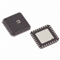
ADN8830ACP-REEL Analog Devices Inc, ADN8830ACP-REEL Datasheet - Page 4

ADN8830ACP-REEL
Manufacturer Part Number
ADN8830ACP-REEL
Description
IC THERMO COOLER CNTRLR 32-LFCSP
Manufacturer
Analog Devices Inc
Datasheet
1.ADN8830ACPZ-REEL7.pdf
(24 pages)
Specifications of ADN8830ACP-REEL
Rohs Status
RoHS non-compliant
Applications
Thermoelectric Cooler
Current - Supply
8mA
Voltage - Supply
3.3 V ~ 5 V
Operating Temperature
-40°C ~ 85°C
Mounting Type
Surface Mount
Package / Case
32-LFCSP
ADN8830
Pin No.
1
2
3
4
5
6
7
8
9
10
11
12
13
14
15
16
17
18
19
20
21
22
23
24
25
26
27
28
29
30
31
32
Mnemonic
THERMFAULT
THERMIN
SD
TEMPSET
TEMPLOCK
NC
VREF
AVDD
OUT B
N2
P2
TEMPCTL
COMPFB
COMPOUT
VLIM
VTEC
COMPSWOUT
COMPSWIN
OUT A
PVDD
P1
N1
PGND
COMPOSC
SYNCIN
FREQ
SOFTSTART
SYNCOUT
PHASE
AGND
TEMPOUT
NC
Digital Output
Type
Analog Input
Digital Input
Analog Input
Digital Output
Analog Output
Power
Analog Input
Analog Output
Analog Output
Analog Output
Analog Input
Analog Output
Analog Input
Analog Output
Analog Output
Analog Input
Analog Input
Power
Digital Output
Digital Output
Ground
Analog Input
Digital Input
Analog Input
Analog Input
Digital Output
Analog Input
Ground
Analog Output
PIN FUNCTION DESCRIPTIONS
Indicates an Open or Short-Circuit Condition from Thermistor.
Thermistor Feedback Input.
Target Temperature Input.
Indicates when Thermistor Temperature is within 0.1 C of Target Tem-
2.5 V Reference Voltage.
Power for Nondriver Sections. 3.0 V min; 5.5 V max.
Drives Linear Output External NMOS Gate.
Drives Linear Output External PMOS Gate.
Output of Error Amplifier. Connects to COMPFB through feedforward
Output of Compensation Amplifier. Connects to COMPFB through feed-
Sets Maximum Voltage across TEC.
Indicates Relative Voltage across the TEC. The 1.5 V corresponds to 0 V
Compensation for Switching Amplifier.
Power for Output Driver Sections. 3.0 V min; 5.5 V max.
Drives PWM Output External PMOS Gate.
Drives PWM Output External NMOS Gate.
Connect as Indicated in the Application Notes Section.
Optional Clock Input. If not connected, clock frequency set by FREQ pin.
Sets Switching Frequency.
Controls Initialization Time for ADN8830 with Capacitor to Ground.
Phase Adjusted Clock Output. Phase set from PHASE pin. Can be used to
Sets Switching and SYNCOUT Clock Phase Relative to SYNCIN Clock.
Analog Ground. Should be low noise for highest accuracy.
Indication of Thermistor Temperature.
No Connection.
Description
Puts Device into Low Current Shutdown Mode. Active low.
perature as Set by TEMPSET Voltage.
No Connection, except as Noted in the Application Notes Section.
Linear Output Feedback. Will typically connect to TEC+ pin of TEC.
section of compensation network.
Feedback Summing Node of Compensation Amplifier. Connects to
TEMPCTL and COMPOUT through compensation network.
back section of compensation network.
across TEC. The 3.0 V indicates maximum output voltage, maximum heat
transfer through TEC.
Compensation for Switching Amplifier. Capacitor connected between
COMPSWIN and COMPSWOUT.
PWM Output Feedback. Will typically connect to TEC– pin of TEC.
Power Ground. External NMOS devices connect to PGND. Can be
connected to digital ground as noise sensitivity at this node is not critical.
drive SYNCIN of other ADN8830 devices.
–4–
REV. C


