LM2635MX National Semiconductor, LM2635MX Datasheet - Page 9
LM2635MX
Manufacturer Part Number
LM2635MX
Description
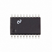
IC REG SYNCH BUCK 5-BIT 20-SOIC
Manufacturer
National Semiconductor
Datasheet
1.LM2635MNOPB.pdf
(13 pages)
Specifications of LM2635MX
Applications
Power Supplies
Current - Supply
2.5mA
Voltage - Supply
4.5 V ~ 5.5 V
Operating Temperature
0°C ~ 125°C
Mounting Type
Surface Mount
Package / Case
20-SOIC (7.5mm Width)
Lead Free Status / RoHS Status
Lead free / RoHS Compliant
Other names
*LM2635MX
LM2635MXTR
LM2635MXTR
Available stocks
Company
Part Number
Manufacturer
Quantity
Price
Company:

Part Number:
LM2635MX
Manufacturer:
FUJITSU
Quantity:
2
Part Number:
LM2635MX
Manufacturer:
NS/国半
Quantity:
20 000
Company:
Part Number:
LM2635MX/NOPB
Manufacturer:
NXP
Quantity:
3 050


Applications Information
The control-to-output transfer function is
The ESR zero frequency is:
The power stage double pole frequency is:
The corresponding Bode plots are shown in Figure 5.
Since the ESR zero frequency is so low, it effectively cancels
the phase shift from one of the power stage poles. This limits
the total phase shift to 90%.
Although this regulator design is stable (phase shift is
when gain = 0dB), it needs compensation to improve the DC
gain and cut off frequency (0dB frequency). Otherwise, the
low DC gain may cause a poor line regulation, and the low
cutoff frequency will hurt transient response performance.
The transfer function for the 2-pole-1-zero compensation
network shown in Figure 4 is:
FIGURE 5. Control-to-Output Bode Plots
(Continued)
10011913
<
90˚
9
where
One of the poles is located at origin to help achieve the
highest DC gain. So there are three parameters to deter-
mine, the position of the zero, the position of the second
pole, and the constant A. To determine the cutoff frequency
and phase margin, the loop bode plots need to be gener-
ated. The loop transfer function is:
By choosing the zero close to the double pole position and
the second pole to half of the switching frequency, the closed
loop transfer function turns out to be very good.
That is, if f
then the cutoff frequency will be 50 kHz, the phase margin
will be 72˚, and the DC gain will be that of the error amplifier.
See Figure 6 below.
The compensation network component values can be deter-
mined by the following equations:
Notice there are three equations but four variables. So one
of the variables can be chosen arbitrarily. Since the current
Z
= 1.32 kHz, f
FIGURE 6. Loop Bode Plots
TF = −TF1 x TF2
P
= 153 kHz, and A = 4.8 x 10
10011917
www.national.com
−6
ΩF,
Related parts for LM2635MX
Image
Part Number
Description
Manufacturer
Datasheet
Request
R

Part Number:
Description:
5-Bit Programmable Synchronous Buck Regulator Controller
Manufacturer:
National Semiconductor
Datasheet:
Part Number:
Description:
National Semiconductor [8-Bit D/A Converter]
Manufacturer:
National Semiconductor
Datasheet:
Part Number:
Description:
National Semiconductor [Media Coprocessor]
Manufacturer:
National Semiconductor
Datasheet:
Part Number:
Description:
Digitally Controlled Tone and Volume Circuit with Stereo Audio Power Amplifier, Microphone Preamp Stage and National 3D Sound
Manufacturer:
National Semiconductor
Datasheet:
Part Number:
Description:
Digitally Controlled Tone and Volume Circuit with Stereo Audio Power Amplifier, Microphone Preamp Stage and National 3D Sound
Manufacturer:
National Semiconductor
Datasheet:
Part Number:
Description:
AC97 Rev 2 Codec with Sample Rate Conversion and National 3D Sound
Manufacturer:
National Semiconductor
Part Number:
Description:
Manufacturer:
National Semiconductor
Datasheet:
Part Number:
Description:
Manufacturer:
National Semiconductor
Datasheet:
Part Number:
Description:
General Purpose, Low Voltage, Low Power, Rail-to-Rail Output Operational Amplifiers
Manufacturer:
National Semiconductor
Datasheet:
Part Number:
Description:
8-bit 20 MSPS flash A/D converter.
Manufacturer:
National Semiconductor
Datasheet:
Part Number:
Description:
Low Noise Quad Operational Amplifier
Manufacturer:
National Semiconductor
Datasheet:
Part Number:
Description:
Quad Differential Line Receivers
Manufacturer:
National Semiconductor
Datasheet:
Part Number:
Description:
Quad High Speed Trapezoidal? Bus Transceiver
Manufacturer:
National Semiconductor
Datasheet:
Part Number:
Description:
Dual Line Receiver
Manufacturer:
National Semiconductor
Datasheet: