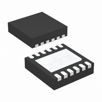
LTC2953CDD-1#PBF Linear Technology, LTC2953CDD-1#PBF Datasheet - Page 3

LTC2953CDD-1#PBF
Manufacturer Part Number
LTC2953CDD-1#PBF
Description
IC PB ON/OFF CONTROLLER 12DFN
Manufacturer
Linear Technology
Datasheet
1.LTC2953CDD-1PBF.pdf
(20 pages)
Specifications of LTC2953CDD-1#PBF
Applications
Push Button, On/Off Controller
Voltage - Supply
2.7 V ~ 27 V
Current - Supply
14µA
Operating Temperature
0°C ~ 70°C
Mounting Type
Surface Mount
Package / Case
12-DFN
Lead Free Status / RoHS Status
Lead free / RoHS Compliant
Voltage - Input
-
Available stocks
Company
Part Number
Manufacturer
Quantity
Price
ELECTRICAL CHARACTERISTICS
SYMBOL
I
V
t
On/Off Timing Pins ( ⎯ P ⎯ B , UVLO, PDT, ⎯ I ⎯ N ⎯ T )
t
I
I
t
t
t
t
t
μP Handshake Pins ( ⎯ K ⎯ I ⎯ L ⎯ L , ⎯ I ⎯ N ⎯ T )
V
V
t
t
t
I
I
V
Power Fail and Voltage Monitor Pins ( ⎯ P ⎯ F ⎯ I , ⎯ P ⎯ F ⎯ O , UVLO, VM, ⎯ R ⎯ S ⎯ T )
V
V
VM
ΔV
V
V
V
V
temperature range, otherwise specifi cations are at T
EN(LKG)
EN, Lock Out
DB, ON
PDT(PU)
PDT(PD)
DB, OFF
PD, Min
PDT
INT
INT, Max
KILL(PD)
KILL, ON BLANK
KILL(LKG)
INT(LKG)
KILL(PW)
EN(VOL)
KILL(TH)
KILL(HYST)
INT(VOL)
PFI(TH)
UVLO(TH)
PFI(HYST)
UVLO(HYST)
PFO(VOL)
RST(VOL)
TH
,
(TH)
Min
PARAMETER
EN/ ⎯ E ⎯ N Leakage Current
EN/ ⎯ E ⎯ N Voltage Output Low
EN/ ⎯ E ⎯ N Lock Out Time (Note 3)
Turn On Debounce Time
PDT Pull Up Current
PDT Pull Down Current
Turn Off Interrupt Debounce Time
Internal ⎯ P ⎯ B Power Down Delay
Time (Note 4)
Additional Adjustable ⎯ P ⎯ B Power
Down Delay Time
Minimum ⎯ I ⎯ N ⎯ T Pulse Width
Maximum ⎯ I ⎯ N ⎯ T Pulse Width
⎯ K ⎯ I ⎯ L ⎯ L Input Threshold Voltage
⎯ K ⎯ I ⎯ L ⎯ L Input Threshold Hysteresis
⎯ K ⎯ I ⎯ L ⎯ L Minimum Pulse Width
⎯ K ⎯ I ⎯ L ⎯ L Propagation Delay
⎯ K ⎯ I ⎯ L ⎯ L Turn On Blanking (Note 5)
⎯ K ⎯ I ⎯ L ⎯ L Leakage Current
⎯ I ⎯ N ⎯ T Leakage Current
⎯ I ⎯ N ⎯ T Output Voltage Low
⎯ P ⎯ F ⎯ I Input Threshold Voltage
UVLO Input Threshold Voltage
Adjustable Reset Threshold
⎯ P ⎯ F ⎯ I -UVLO Threshold Mismatch
⎯ P ⎯ F ⎯ I Input Hysteresis
UVLO Input Hysteresis
⎯ P ⎯ F ⎯ O Output Voltage Low
⎯ R ⎯ S ⎯ T Output Voltage Low
CONDITIONS
V
V
I
Enable Released → Enable Asserted
⎯ P ⎯ B Falling → Enable Asserted
V
V
⎯ P ⎯ B , UVLO Falling → ⎯ I ⎯ N ⎯ T Falling
⎯ P ⎯ B , UVLO Falling → Enable Released
PDT Open
C
⎯ I ⎯ N ⎯ T Asserted → ⎯ I ⎯ N ⎯ T Released
C
⎯ K ⎯ I ⎯ L ⎯ L Falling
⎯ K ⎯ I ⎯ L ⎯ L Falling → Enable Released
⎯ K ⎯ I ⎯ L ⎯ L = Low, Enable Asserted → Enable Released
V
V
I
Falling
Falling
Falling/Rising
I
I = 3mA
EN/ ⎯ E ⎯ N
INT
PFO
EN/ ⎯ E ⎯ N
EN/ ⎯ E ⎯ N
PDT
PDT
PDT
PDT
KILL
INT
= 3mA
= 500μA
= 3V
= 0V
= 1.3V
= 1500pF
= 1500pF, ⎯ I ⎯ N ⎯ T Asserted → ⎯ I ⎯ N ⎯ T Released
A
= 0.6V
= 500μA
= 1V, Sink Current Off
= 40V, Sink Current Off
= 25°C. V
The
●
IN
denotes the specifi cations which apply over the full operating
= 2.7V to 27V, unless otherwise noted (Note 2).
●
●
●
●
●
●
●
●
●
●
●
●
●
●
●
●
●
●
●
●
●
●
●
●
●
●
●
●
–2.4
0.57
MIN
400
492
492
492
2.4
52
26
26
52
26
35
10
30
–5
30
9
2
0.11
11.5
43.5
0.11
0.11
0.11
TYP
512
500
500
500
0.6
64
32
–3
32
64
32
30
50
3
0
4
LTC2953
MAX
±0.1
–3.6
13.5
54.5
0.63
±0.1
±0.1
650
508
508
508
0.4
3.6
0.4
0.4
0.4
±1
82
41
41
82
41
50
30
10
70
5
UNITS
3
2953f
mV
mV
mV
mV
mV
mV
mV
ms
ms
ms
ms
ms
ms
ms
ms
μA
μA
μA
μA
μA
μA
μs
μs
V
V
V
V
V


