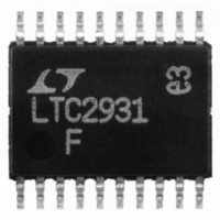
LTC2931CF#PBF Linear Technology, LTC2931CF#PBF Datasheet - Page 7

LTC2931CF#PBF
Manufacturer Part Number
LTC2931CF#PBF
Description
IC 6 PWR SUPPLY MONITOR 20TSSOP
Manufacturer
Linear Technology
Datasheet
1.LTC2931CFPBF.pdf
(16 pages)
Specifications of LTC2931CF#PBF
Applications
Six Power Supply Monitor
Voltage - Supply
1 V ~ 7 V
Operating Temperature
0°C ~ 70°C
Mounting Type
Surface Mount
Package / Case
20-TSSOP
Lead Free Status / RoHS Status
Lead free / RoHS Compliant
Current - Supply
-
Voltage - Input
-
Available stocks
Company
Part Number
Manufacturer
Quantity
Price
PIN FUNCTIONS
COMP5 (Pin 1): Comparator Output 5. Real-time logic
output with weak 6μA pull-up to V2. Pulls high when V5
is above reset threshold. May be pulled greater than V2
using external pull-up. Leave open if unused.
V5 (Pin 2): Adjustable Voltage Input 5. High impedance
comparator input with 0.5V typical threshold. See
Applications Information for details. Tie to V1 if unused.
COMP3 (Pin 3): Comparator Output 3. Real-time logic
output with weak 6μA pull-up to V2. Pulls high when V3
is above its reset threshold. May be pulled greater than
V2 using external pull-up. Leave open if unused.
COMP1 (Pin 4): Comparator Output 1. Real-time logic
output with weak 6μA pull-up to V2. Pulls high when V1
is above its reset threshold. May be pulled greater than
V2 using external pull-up. Leave open if unused.
V3 (Pin 5): Voltage Input 3. Select from 2.5V, 1.8V, 1.5V,
or ADJ. See Applications Information for details. Tie to
V1 if unused.
V1 (Pin 6): Voltage Input 1. Select from 5V or 3.3V. See
Applications Information for details. The greater of V1 or
V2 is also V
with a 0.1μF (or greater) capacitor.
CRT (Pin 7): Reset Timeout Capacitor. Attach an external
capacitor (C
Leaving the pin open generates a minimum delay of
approximately 25μs. A 47nF capacitor generates a 94ms
reset delay time.
RST (Pin 8): Reset Output. Logic output with weak 6μA
pull-up to V2. Pulls low when any voltage input is below
the reset threshold and held low for the confi gured delay
time after all voltage inputs are above threshold. May be
pulled greater than V2 using external pull-up. Leave open
if unused.
WDO (Pin 9): Watchdog Output. Logic output with weak
6μA pull-up to V2. May be pulled greater than V2 using
external pull-up. The watchdog timer is enabled when RST
is high. The watchdog output pulls low if the watchdog timer
times out and remains low for one reset timeout period.
The watchdog output is cleared with a WDI transition or
anytime RST is low.The output will toggle between high
CC
RT
) to GND to set a reset timeout of 2ms/nF .
for the device. Bypass this pin to ground
and low as long as the watchdog and reset timers are
allowed to time out. Leave open if unused.
WDI (Pin 10): Watchdog Input. A logic input whose rising
or falling edge must occur on this pin (while RST is high)
within the selected watchdog time-out period, prohibiting
a high-to-low transition on the WDO pin. The capacitor
attached to the CWT pin sets the watchdog time-out period.
A rising or falling edge on the WDI pin clears the voltage
on the C
WDI to V1 or GND if unused. Tie CWT to GND to disable
the watchdog function.
CWT (Pin 11): Watchdog Timeout Capacitor. Attach
a capacitor (C
watchdog time-out period of 20ms/nF . Leaving the pin open
generates a minimum timeout of approximately 200μs.
A 47nF capacitor generates a 940ms watchdog time-out
period. Tie CWT to GND to disable the watchdog function.
GND (Pin 12): Ground.
VPG (Pin 13): Threshold Select Input. Connect to an
external 1% resistive divider between VREF and GND to
select 1 of 16 combinations and/or ±adjustable voltage
thresholds (See Table 1). Do not add capacitance on the
VPG pin.
VREF (Pin 14): Buffered Reference Voltage Output. A
1.210V nominal reference used for the mode selection
voltage (V
applications. The buffered reference can source and sink
up to 1mA. The reference can drive a bypass capacitor of
up to 1000pF without oscillation.
V4 (Pin 15): Voltage Input 4. Select from 1.8V, 1.5V, ADJ
or –ADJ. See Applications Information for details. Tie to
V1 if unused and confi gured for positive voltage.
V2 (Pin 16): Voltage Input 2. Select from 3.3V, 3V or 2.5V.
See Applications Information for details. The greater of V1,
V2 is also V
with a 0.1μF (or greater) capacitor. All status outputs are
weakly pulled up to V2.
COMP4 (Pin 17): Comparator Output 4. Real-time logic
output with weak 6μA pull-up to V2. Pulls high when V4
is above its reset threshold. May be pulled greater than
V2 using external pull-up. Leave open if unused.
WT
PG
capacitor, preventing WDO from going low. Tie
CC
) and for the offset of negative adjustable
for the device. Bypass this pin to ground
WT
) between CWT and GND to set a
LTC2931
2931fb
7


