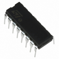
L6599N STMicroelectronics, L6599N Datasheet - Page 29

L6599N
Manufacturer Part Number
L6599N
Description
IC RESONANT CONVERTR CTRLR 16DIP
Manufacturer
STMicroelectronics
Type
Phase Shift Resonant Controllerr
Datasheet
1.L6599DTR.pdf
(36 pages)
Specifications of L6599N
Applications
Resonant Converter Controller
Voltage - Supply
8.85 V ~ 16 V
Current - Supply
3.5mA
Operating Temperature
0°C ~ 105°C
Mounting Type
Through Hole
Package / Case
16-DIP (0.300", 7.62mm)
Number Of Pwm Outputs
1
Switching Freq
500KHz
Operating Supply Voltage (max)
16V
Output Current
800A
Operating Temperature Classification
Automotive
Mounting
Through Hole
Pin Count
16
Package Type
PDIP
Number Of Outputs
Single Output
Switching Frequency
500 KHz
Operating Supply Voltage
8.85 V to 16 V
Maximum Operating Temperature
+ 150 C
Minimum Operating Temperature
- 40 C
Mounting Style
Through Hole
Supply Voltage Range
8.85V To 16V
Digital Ic Case Style
DIP
No. Of Pins
16
Operating Temperature Range
-40°C To +150°C
Svhc
No SVHC (15-Dec-2010)
Base Number
6599
Device Type
Power
Rohs Compliant
Yes
For Use With
497-10542 - BOARD EVAL BASED ON L6599497-8429 - BOARD ADAPTER L6599/STP12NM50N497-8265 - BOARD EVAL BASED ON L6599497-5857 - DEMO BOARD FOR L6599497-5856 - DEMO BOARD FOR L6599497-5497 - EVAL BOARD FOR L6599497-5496 - EVAL BOARD FOR L6599
Lead Free Status / RoHS Status
Lead free / RoHS Compliant
Voltage - Input
-
Lead Free Status / Rohs Status
Compliant
Other names
497-5723
L6599NR
L6599NR
Available stocks
Company
Part Number
Manufacturer
Quantity
Price
L6599
7.7
voltage on the pin exceeds 7 V the device is shutdown. If its supply voltage is always above
the UVLO threshold, the IC will restart as the voltage falls below 7 V.
The LINE pin, while the device is operating, is a high impedance input connected to high
value resistors, thus it is prone to pick up noise, which might alter the OFF threshold or give
origin to undesired switch-off of the IC during ESD tests. It is possible to bypass the pin to
ground with a small film capacitor (e.g. 1-10 nF) to prevent any malfunctioning of this kind. If
the function is not used the pin has to be connected to a voltage greater than 1.25 V but
lower than 6V (worst-case value of the 7 V threshold).
Bootstrap section
The supply of the floating high-side section is obtained by means of a bootstrap circuitry.
This solution normally requires a high voltage fast recovery diode to charge the bootstrap
capacitor C
It is realized by means of a high voltage DMOS, working in the third quadrant and driven
synchronously with the low side driver (LVG), with a diode in series to the source, as shown
in
Figure 34. Bootstrap supply: internal bootstrap synchronous diode
The diode prevents any current can flow from the VBOOT pin back to V
supply is quickly turned off when the internal capacitor of the pump is not fully discharged.
To drive the synchronous DMOS it is necessary a voltage higher than the supply voltage
V
The bootstrap structure introduces a voltage drop while recharging C
side driver is on), which increases with the operating frequency and with the size of the
external power MOSFET. It is the sum of the drop across the R
across the series diode. At low frequency this drop is very small and can be neglected but,
as the operating frequency increases, it must be taken into account. In fact, the drop
reduces the amplitude of the driving signal and can significantly increase the R
external high-side MOSFET and then its conductive loss.
CC
Figure 34.
. This voltage is obtained by means of an internal charge pump
BOOT
Vcc
. In the L6599 a patented integrated structure, replaces this external diode.
12
LVG
L6599
16
14
OUT
VBOOT
DS(on)
Application information
(Figure
BOOT
C
and the forward drop
BOOT
CC
(i.e. when the low
in case that the
34).
DS(on)
of the
29/36


