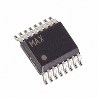
MAX1864TEEE+ Maxim Integrated Products, MAX1864TEEE+ Datasheet - Page 10

MAX1864TEEE+
Manufacturer Part Number
MAX1864TEEE+
Description
IC PWR SUPPLY CONTROLLER 16QSOP
Manufacturer
Maxim Integrated Products
Datasheet
1.MAX1864TEEE.pdf
(25 pages)
Specifications of MAX1864TEEE+
Applications
Power Supply Controller
Voltage - Input
4.5 ~ 28 V
Current - Supply
1mA
Operating Temperature
-40°C ~ 85°C
Mounting Type
Surface Mount
Package / Case
16-QSOP
Lead Free Status / RoHS Status
Lead free / RoHS Compliant
Voltage - Supply
-
Lead Free Status / Rohs Status
Lead free / RoHS Compliant
xDSL/Cable Modem Triple/Quintuple Output
Power Supplies
The MAX1864/MAX1865 power-supply controllers pro-
vide system power for cable and xDSL modems. The
main step-down DC-DC controller operates in a cur-
rent-mode pulse-width-modulation (PWM) control
scheme to ease compensation requirements and pro-
vide excellent load- and line-transient response.
The MAX1864 includes two analog gain blocks to regu-
late two additional positive auxiliary output voltages,
and the MAX1865 includes four analog gain blocks to
regulate three additional positive and one negative aux-
iliary output voltages. The positive regulator gain blocks
can be used to generate low-voltage rails directly from
the main step-down converter or higher voltages using
coupled windings from the step-down converter. The
negative gain block can be used in conjunction with a
coupled winding to generate -5V, -12V, or -15V.
The MAX1864/MAX1865 step-down converters use a
pulse-width-modulated (PWM) current-mode control
scheme (Figure 2). An internal transconductance
amplifier establishes an integrated error voltage at the
COMP pin. The heart of the current-mode PWM con-
troller is an open-loop comparator that compares the
10
MAX1864
______________________________________________________________________________________
10
11
12
13
14
15
16
9
PIN
MAX1865
13
14
15
16
17
18
19
20
Detailed Description
NAME
GND
ILIM
BST
DH
DL
LX
VL
IN
DC-DC Controller
Dual Mode Current-Limit Adjustment Input. Connect to VL for the default 250mV
current-limit threshold. In adjustable mode, the current-limit threshold voltage is 1/5th
the voltage present at ILIM. Connect to a resistive-divider between VL and GND to
adjust V
default value is approximately VL - 1V.
Ground
Low-Side Gate-Driver Output. DL swings between GND and VL.
Inductor Connection. Used for current sense between IN and LX, and used for current
limit between LX and GND.
High-Side Gate-Driver Output. DH swings between LX and BST.
Boost Flying Capacitor Connection. Connect BST to the external boost diode and
capacitor as shown in the standard application circuit (Figures 1 and 6).
Internal 5V Linear-Regulator Output. Supplies the IC and powers the DL low-side gate
driver and external boost diode and capacitor. Bypass with a 1µF or greater ceramic
capacitor to GND.
Input Supply Voltage, 4.5V to 28V. Bypass to GND with a 1µF or greater ceramic
capacitor close to the IC.
ILIM
between 1V and 2.5V. The logic threshold for switchover to the 250mV
integrated voltage-feedback signal against the ampli-
fied current-sense signal plus the slope compensation
ramp. At each rising edge of the internal clock, the
high-side MOSFET turns-on until the PWM comparator
trips or the maximum duty cycle is reached. During this
on-time, current ramps up through the inductor, sourc-
ing current to the output and storing energy in a mag-
netic field. The current-mode feedback system
regulates the peak inductor current as a function of the
output voltage error signal. Since the average inductor
current is nearly the same as the peak inductor current
(assuming that the inductor value is relatively high to
minimize ripple current), the circuit acts as a switch-
mode transconductance amplifier. It pushes the output
LC filter pole, normally found in a voltage-mode PWM,
to a higher frequency. To preserve inner loop stability
and eliminate inductor stair-casing, a slope-compensa-
tion ramp is summed into the main PWM comparator.
During the second-half of the cycle, the high-side MOS-
FET turns off and the low-side N-channel MOSFET turns
on. Now the inductor releases the stored energy as its
current ramps down, providing current to the output.
Therefore, the output capacitor stores charge when the
inductor current exceeds the load current and dis-
charges when the inductor current is lower, smoothing
FUNCTION
Pin Description (continued)


