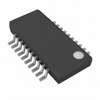
MAX1865TEEP+ Maxim Integrated Products, MAX1865TEEP+ Datasheet - Page 13

MAX1865TEEP+
Manufacturer Part Number
MAX1865TEEP+
Description
IC PWR SUPPLY CONTROLLER 20QSOP
Manufacturer
Maxim Integrated Products
Datasheet
1.MAX1864TEEE.pdf
(25 pages)
Specifications of MAX1865TEEP+
Applications
Power Supply Controller
Voltage - Input
4.5 ~ 28 V
Current - Supply
1.4mA
Operating Temperature
-40°C ~ 85°C
Mounting Type
Surface Mount
Package / Case
20-QSOP
Lead Free Status / RoHS Status
Lead free / RoHS Compliant
Voltage - Supply
-
Lead Free Status / Rohs Status
Lead free / RoHS Compliant
The current-limit circuit employs a unique “valley” cur-
rent-limiting algorithm that uses the low-side MOSFET’s
on-resistance as a sensing element (Figure 3). If the
voltage across the low-side MOSFET (R
DUCTOR
beginning of a new oscillator cycle, the MAX1864/
MAX1865 will not turn on the high-side MOSFET. The
actual peak current is greater than the current-limit
threshold by an amount equal to the inductor ripple
current. Therefore, the exact current-limit characteristic
and maximum load capability are a function of the low-
side MOSFET on-resistance, inductor value, input volt-
age, and output voltage. The reward for this uncertainty
is robust, loss-less overcurrent limiting.
In adjustable mode, the current-limit threshold voltage
is 1/5th the voltage seen at ILIM (I
Adjust the current-limit threshold by connecting a resis-
tive-divider from VL to ILIM to GND. The current-limit
threshold can be set from 106mV to 530mV, which cor-
responds to ILIM input voltages of 500mV to 2.5V. This
adjustable current limit accommodates MOSFETs with
a wide range of on-resistance characteristics (see
Design Procedure). The current-limit threshold defaults
to 250mV when ILIM is connected to VL. The logic
threshold for switchover to the 250mV default value is
approximately VL - 1V.
Carefully observe the PC board layout guidelines to
ensure that noise and DC errors don’t corrupt the cur-
rent-sense signals seen by LX and GND. The IC must
be mounted close to the low-side MOSFET with short
(less than 5mm), direct traces making a Kelvin sense
connection.
Synchronous rectification reduces conduction losses in
the rectifier by replacing the normal Schottky catch
diode with a low-resistance MOSFET switch. The
MAX1864/MAX1865 also use the synchronous rectifier
to ensure proper startup of the boost gate-driver circuit
and to provide the current-limit signal.
The DL low-side drive waveform is always the comple-
ment of the DH high-side drive waveform (with con-
trolled dead time to prevent cross-conduction or
“shoot-through”). A dead-time circuit monitors the DL
output and prevents the high-side FET from turning on
until DL is fully off. For the dead-time circuit to work
properly, there must be a low-resistance, low-induc-
tance path from the DL driver to the MOSFET gate.
Otherwise, the sense circuitry in the MAX1864/
MAX1865 will interpret the MOSFET gate as “off” when
gate charge actually remains. Use very short, wide
) exceeds the current-limit threshold at the
xDSL/Cable Modem Triple/Quintuple Output
______________________________________________________________________________________
Synchronous Rectifier Driver (DL)
Current-Limit Circuit
VALLEY
= 0.2
DS(ON)
✕
V
✕
ILIM
I
IN-
).
traces (50mil to 100mil wide if the MOSFET is 1 inch
from the device). The dead time at the other edge (DH
turning off) is determined by a fixed internal delay.
Gate-drive voltage for the high-side N-channel switch is
generated by a flying-capacitor boost circuit (Figure 1).
The capacitor between BST and LX is alternately
charged from the VL supply and placed parallel to the
high-side MOSFET’s gate-source terminals.
On startup, the synchronous rectifier (low-side MOS-
FET) forces LX to ground and charges the boost
capacitor to 5V. On the second half-cycle, the switch-
mode power supply turns on the high-side MOSFET by
closing an internal switch between BST and DH. This
provides the necessary gate-to-source voltage to turn
on the high-side switch, an action that boosts the 5V
gate-drive signal above the battery voltage.
All MAX1864/MAX1865 functions, except the current-
sense amplifier, are internally powered from the on-
chip, low-dropout 5V regulator. The maximum regulator
input voltage (V
(VL) with at least a 1µF ceramic capacitor to GND. The
V
V
The internal linear regulator can source up to 20mA to
supply the IC, power the low-side gate driver, charge
the external boost capacitor, and supply small external
loads. When driving particularly large FETs, little or no
regulator current may be available for external loads.
For example, when switched at 200kHz, a large FET
with 40nC total gate charge requires 40nC x 200kHz,
or 8mA.
Figure 3. “Valley” Current-Limit Threshold Point
IN
IN
-to-VL dropout voltage is typically 200mV, so when
is less than 5.2V, VL is typically V
Internal 5V Linear Regulator (VL)
IN
) is 28V. Bypass the regulator’s output
Power Supplies
High-Side Gate-Drive Supply (BST)
TIME
I
PEAK
= I
VALLEY
+
[
(V
IN
IN
- V
L
- 200mV.
OUT
)
( )
V
V
IN
OUT
f
OSC
]
-I
I
I
PEAK
LOAD
VALLEY
13


