AD637JQ Analog Devices Inc, AD637JQ Datasheet - Page 8
AD637JQ
Manufacturer Part Number
AD637JQ
Description
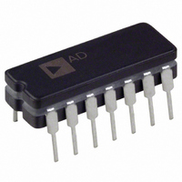
IC RMS/DC CONV PRECISION 14-CDIP
Manufacturer
Analog Devices Inc
Specifications of AD637JQ
Rohs Status
RoHS non-compliant
Current - Supply
2.2mA
Voltage - Supply
±3.0V ~ 18V
Mounting Type
Through Hole
Package / Case
14-CDIP (0.300", 7.62mm)
Accuracy %
0.25%
Bandwidth
200kHz
Supply Current
2.2mA
Power Dissipation Pd
108mW
Supply Voltage Range
± 3V To ± 18V
Digital Ic Case Style
DIP
No. Of Pins
14
Input Type
RMS
Module Type
Converter
Output Type
DC
Voltage, Supply
± 18 VDC
For Use With
AD637-EVALZ - BOARD EVALUATION FOR AD637
Lead Free Status / RoHS Status
Contains lead / RoHS non-compliant
Available stocks
Company
Part Number
Manufacturer
Quantity
Price

Part Number:
AD637JQ
Manufacturer:
ADI/亚德诺
Quantity:
20 000
Company:
Part Number:
AD637JQZ
Manufacturer:
NS
Quantity:
6 221


STANDARD CONNECTION
The AD637 is simple to connect for a majority of rms
measurements. In the standard rms connection shown in
Figure 5, only a single external capacitor is required to set the
averaging time constant. In this configuration, the AD637
computes the true rms of any input signal. An averaging error,
the magnitude of which is dependent on the value of the
averaging capacitor, is present at low frequencies. For example,
if the filter capacitor, C
increases to 1% at 3 Hz. To measure ac signals, the AD637 can
be ac-coupled through the addition of a nonpolar capacitor in
series with the input, as shown in Figure 5.
4.7kΩ
The performance of the AD637 is tolerant of minor variations
in the power supply voltages; however, if the supplies used
exhibit a considerable amount of high frequency ripple, it is
advisable to bypass both supplies to ground through a 0.1 µF
ceramic disc capacitor placed as close to the device as possible.
The output signal range of the AD637 is a function of the
supply voltages, as shown in Figure 6. The output signal can be
used buffered or nonbuffered, depending on the characteristics
of the load. If no buffer is needed, tie the buffer input (Pin 1) to
common. The output of the AD637 is capable of driving 5mA
into a 2 kΩ load without degrading the accuracy of the device.
+V
S
1
2 NC
3 COM
4
5
6
7
BUF IN
OUT
OFF
CS
DEN
IN
DB OUT
Figure 5. Standard RMS Connection
25kΩ
BIAS
AV
, is 4 µF, the error is 0.1% at 10 Hz and
SQUARER/
AD637
DIVIDER
ABSOLUTE
VALUE
25kΩ
BUFFER
OUT
+V
C
–V
V
NC
AV
IN
S
S
14
NC
13
12
11
10
9
8
+
(OPTIONAL)
C
AV
+V
–V
V
OUT
S
S
V
Rev. G | Page 9 of 20
IN
= V
IN
2
CHIP SELECT
The AD637 includes a chip select feature that allows the user to
decrease the quiescent current of the device from 2.2 mA to
350 µA. This is done by driving the CS, Pin 5, to below 0.2 V dc.
Under these conditions, the output goes into a high impedance
state. In addition to lowering power consumption, this feature
permits bussing the outputs of a number of AD637s to form a
wide bandwidth rms multiplexer. If the chip select is not being
used, Pin 5 should be tied high.
OPTIONAL TRIMS FOR HIGH ACCURACY
The AD637 includes provisions for trimming out output offset
and scale factor errors resulting in significant reduction in the
maximum total error, as shown in Figure 7. The residual error is
due to a nontrimmable input offset in the absolute value circuit
and the irreducible nonlinearity of the device.
Referring to Figure 8, the trimming process follows:
• Offset trim: Ground the input signal, V
• Scale factor trim: Resistor R4 is inserted in series with
to give 0 V output from Pin 9. Alternatively, R1 can be
adjusted to give the correct output with the lowest expected
value of V
the input to lower the range of the scale factor. Connect
the desired full-scale input to V
calibrated ac signal, and trim R3 to give the correct output
at Pin 9, that is, 1 V dc should give l.000 V dc output. Of
course, a 2 V p-p sine wave should give 0.707 V dc output.
Remaining errors are due to the nonlinearity.
20
15
10
5
0
0
Figure 6. AD637 Maximum V
IN
.
± 3
SUPPLY VOLTAGE – DUAL SUPPLY (V)
± 5
± 10
IN
OUT
, using either a dc or a
vs. Supply Voltage
IN
, and adjust R1
± 15
AD637
± 18
Related parts for AD637JQ
Image
Part Number
Description
Manufacturer
Datasheet
Request
R

Part Number:
Description:
BOARD EVALUATION FOR AD637
Manufacturer:
Analog Devices Inc
Datasheet:

Part Number:
Description:
±1.7g Dual-Axis IMEMS Accelerometer Evaluation Board
Manufacturer:
Analog Devices Inc
Datasheet:
Part Number:
Description:
Inertial Sensor Evaluation System
Manufacturer:
Analog Devices Inc
Datasheet:
Part Number:
Description:
Manufacturer:
Analog Devices Inc
Datasheet:
Part Number:
Description:
Manufacturer:
Analog Devices Inc
Datasheet:
Part Number:
Description:
Manufacturer:
Analog Devices Inc
Datasheet:
Part Number:
Description:
Manufacturer:
Analog Devices Inc
Datasheet:
Part Number:
Description:
Manufacturer:
Analog Devices Inc
Datasheet:
Part Number:
Description:
Manufacturer:
Analog Devices Inc
Datasheet:
Part Number:
Description:
Manufacturer:
Analog Devices Inc
Datasheet:
Part Number:
Description:
Manufacturer:
Analog Devices Inc
Datasheet:
Part Number:
Description:
Manufacturer:
Analog Devices Inc
Datasheet:
Part Number:
Description:
Manufacturer:
Analog Devices Inc
Datasheet: