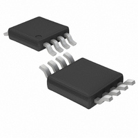
LTC1966CMS8#TRPBF Linear Technology, LTC1966CMS8#TRPBF Datasheet - Page 11

LTC1966CMS8#TRPBF
Manufacturer Part Number
LTC1966CMS8#TRPBF
Description
IC PREC RMS/DC CONV MCRPWR 8MSOP
Manufacturer
Linear Technology
Specifications of LTC1966CMS8#TRPBF
Current - Supply
155µA
Voltage - Supply
2.7 V ~ 5.5 V
Mounting Type
Surface Mount
Package / Case
8-MSOP, Micro8™, 8-uMAX, 8-uSOP,
Lead Free Status / RoHS Status
Lead free / RoHS Compliant
Available stocks
Company
Part Number
Manufacturer
Quantity
Price
APPLICATIO S I FOR ATIO
Unlike the prior generation RMS-to-DC converters, the
LTC1966 computation does NOT use log/antilog circuits,
which have all the same problems, and more, of log/
antilog multipliers/dividers, i.e., linearity is poor, the band-
width changes with the signal amplitude and the gain drifts
with temperature.
How an RMS-to-DC Converter Works
Monolithic RMS-to-DC converters use an implicit com-
putation to calculate the RMS value of an input signal. The
fundamental building block is an analog multiply/divide
used as shown in Figure 3. Analysis of this topology is
easy and starts by identifying the inputs and the output of
the lowpass filter. The input to the LPF is the calculation
from the multiplier/divider; (V
filter will take the average of this to create the output,
mathematically:
Because V
V
V
V
Figure 3. RMS-to-DC Converter with Implicit Computation
V
OUT
OUT
OUT
V
OUT
V
OUT
IN
2
2
V
IN
V
V
V
V
OUT
V
OUT
OUT
IN
IN
V
IN
IN
V
2
V
2
2
is DC,
OUT
IN
2
U
,
,
,
2
or
and
RMS V
,
U
so
IN
V
V
OUT
IN
LPF
IN
2
)
2
W
/V
OUT
1966 F03
. The lowpass
V
OUT
U
The
duty cycle (D) will be proportional to the ratio of the input
signal divided by the output. The
modulator with excellent linearity. The single-bit output is
used to selectively buffer or invert the input signal. Again,
this is a circuit with excellent linearity, because it operates
at only two points: 1 gain; the average effective multipli-
cation over time will be on the straight line between these
two points. The combination of these two elements again
creates a lowpass filter input signal equal to (V
which, as shown above, results in RMS-to-DC conversion.
The lowpass filter performs the averaging of the RMS
function and must be a lower corner frequency than the
lowest frequency of interest. For line frequency measure-
ments, this filter is simply too large to implement on-chip,
but the LTC1966 needs only one capacitor on the output to
implement the lowpass filter. The user can select this
capacitor depending on frequency range and settling time
requirements, as will be covered in the Design Cookbook
section to follow.
This topology is inherently more stable and linear than log/
antilog implementations primarily because all of the signal
processing occurs in circuits with high gain op amps
operating closed loop.
V
How the LTC1966 RMS-to-DC Converter Works
The LTC1966 uses a completely new topology for RMS-to-
DC conversion, in which a
divider, and a simple polarity switch is used as the multi-
plier
1
Multiple patents pending
IN
1
as shown in Figure 4.
modulator has a single-bit output whose average
-
Figure 4. Topology of LTC1966
REF
D
1
V
V
OUT
IN
modulator acts as the
LPF
is a 2nd order
LTC1966
IN
sn1966 1966fas
)
11
2
/V
V
OUT
OUT
,


