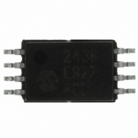
MCP98243-BE/ST Microchip Technology, MCP98243-BE/ST Datasheet - Page 11

MCP98243-BE/ST
Manufacturer Part Number
MCP98243-BE/ST
Description
IC TEMP SENSOR 3V 2WIRE 8-TSSOP
Manufacturer
Microchip Technology
Specifications of MCP98243-BE/ST
Package / Case
8-TSSOP
Output Type
I²C™/SMBus™
Function
Temp Monitoring System (Sensor)
Topology
ADC (Sigma Delta), Register Bank
Sensor Type
Internal
Sensing Temperature
-40°C ~ 125°C
Output Alarm
No
Output Fan
Yes
Voltage - Supply
2.7 V ~ 5.5 V
Operating Temperature
-40°C ~ 125°C
Mounting Type
Surface Mount
Temperature Threshold
+ 125 C
Full Temp Accuracy
1 C
Digital Output - Bus Interface
2-Wire, SMBus, I2C
Digital Output - Number Of Bits
8 bit
Supply Voltage (max)
6 V
Supply Voltage (min)
1.8 V
Description/function
Thermal Management ICs
Maximum Operating Temperature
+ 125 C
Minimum Operating Temperature
- 40 C
Supply Current
100 uA to 1100 uA
Ic Output Type
Digital
Sensing Accuracy Range
± 0.5°C
Temperature Sensing Range
-40°C To +125°C
Supply Voltage Range
2.7V To 5.5V
Sensor Case Style
TSSOP
No. Of Pins
8
Rohs Compliant
Yes
Resolution (bits)
8bit
Supply Voltage Min
3V
Lead Free Status / RoHS Status
Lead free / RoHS Compliant
Lead Free Status / RoHS Status
Lead free / RoHS Compliant, Lead free / RoHS Compliant
Available stocks
Company
Part Number
Manufacturer
Quantity
Price
Company:
Part Number:
MCP98243-BE/ST
Manufacturer:
MICROCHIP
Quantity:
12 000
Part Number:
MCP98243-BE/ST
Manufacturer:
MICROCHIP/微芯
Quantity:
20 000
3.0
The descriptions of the pins are listed in
TABLE 3-1:
3.1
These pins are device address input pins.
The address pins correspond to the Least Significant
bits (LSb) of address bits. The Most Significant bits
(MSb) (A6, A5, A4, A3). This is shown in
TABLE 3-2:
The A0 Address pin is a multi-function pin. This input
pin is also used for high voltge input V
EEPROM Software Write Protect feature, see 5.3.3
“Write Protection”.
All address pin have an internal pull-down resistors.
3.2
The GND pin is the system ground pin.
3.3
SDA is a bidirectional input/output pin, used to serially
transmit data to/from the host controller. This pin
requires a pull-up resistor. (See Section 4.0 “Serial
Communication”).
© 2009 Microchip Technology Inc.
Sensor
EEPROM
EEPROM
Write Protect
DFN/TDFN/
Note:
UDFN
Device
1
2
3
4
5
6
7
8
9
PIN DESCRIPTION
Address Pins (A0, A1, A2)
Ground Pin (GND)
Serial Data Line (SDA)
User-selectable address is shown by X.
PIN FUNCTION TABLES
MCP98243 ADDRESS BYTE
A6
0
1
0
TSSOP
Address Code
—
1
2
3
4
5
6
7
8
A5
0
0
1
A4
1
1
1
A3
1
0
0
Symbol
Event
GND
HV
SDA
SCL
V
EP
A0
A1
A2
A2
DD
X
Table
Table
to enable the
Address
Slave
A1
X
3-1.
3-2.
A0
X
Slave Address and EEPROM Software Write Protect high voltage
input (V
Slave Address
Slave Address
Ground
Serial Data Line
Serial Clock Line
Temperature Alert Output
Power Pin
Exposed Thermal Pad (EP); must be connected to GND.
HV
)
3.4
The SCL is a clock input pin. All communication and
timing is relative to the signal on this pin. The clock is
generated by the host or master controller on the bus.
(See Section 4.0 “Serial Communication”).
3.5
The MCP98243 temperature Event output pin is an
open-drain output. The device outputs a signal when
the ambient temperature goes beyond the user-pro-
grammed temperature limit. (see Section 5.2.3 “Event
Output Configuration”).
3.6
V
specified in the DC electrical specification table, is
applied on this pin.
3.7
There is an internal electrical connection between the
Exposed Thermal Pad (EP) and the GND pin; they
must be connected to the same potential on the Printed
Circuit Board (PCB).
DD
is the power pin. The operating voltage range, as
Serial Clock Line (SCL)
Temperature Alert, Open-Drain
Output (Event)
Power Pin (V
Exposed Thermal Pad (EP)
Pin Function
DD
MCP98243
)
DS22153A-page 11


