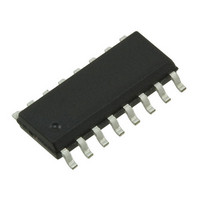
MAX6693UP9A+ Maxim Integrated Products, MAX6693UP9A+ Datasheet - Page 10

MAX6693UP9A+
Manufacturer Part Number
MAX6693UP9A+
Description
IC TEMP MONITOR 7CH 20-TSSOP
Manufacturer
Maxim Integrated Products
Datasheet
1.MAX6693UP9A.pdf
(19 pages)
Specifications of MAX6693UP9A+
Function
Temp Monitoring System (Sensor)
Topology
ADC, Buffer, Multiplexer, Register Bank
Sensor Type
External & Internal
Sensing Temperature
-40°C ~ 125°C, External Sensor
Output Type
SMBus™
Output Alarm
Yes
Output Fan
Yes
Voltage - Supply
3 V ~ 3.6 V
Operating Temperature
-40°C ~ 125°C
Mounting Type
Surface Mount
Package / Case
20-TSSOP
Lead Free Status / RoHS Status
Lead free / RoHS Compliant
7-Channel Precision Temperature Monitor
with Beta Compensation
If a channel’s input DXP_ and DXN_ are left open, the
MAX6693 detects a diode fault. An open diode fault does
not cause either ALERT or OVERT to assert. A bit in the sta-
tus register for the corresponding channel is set to 1 and the
temperature data for the channel is stored as all 1s (FFh). It
takes approximately 4ms for the MAX6693 to detect a diode
fault. Once a diode fault is detected, the MAX6693 goes to
the next channel in the conversion sequence.
There are 11 alarm threshold registers that store over-tem-
perature ALERT and OVERT threshold values. Seven of
these registers are dedicated to storing one local alert tem-
perature threshold limit and six remote alert temperature
threshold limits (see the ALERT Interrupt Mode section).
The remaining four registers are dedicated to remote chan-
nels 1, 4, 5, and 6 to store overtemperature threshold limits
Figure 3. SMBus Write-Timing Diagram
Figure 4. SMBus Read-Timing Diagram
10
SMBCLK
SMBDATA
SMBCLK
SMBDATA
A = START CONDITION.
B = MSB OF ADDRESS CLOCKED INTO SLAVE.
C = LSB OF ADDRESS CLOCKED INTO SLAVE.
D = R/W BIT CLOCKED INTO SLAVE.
E = SLAVE PULLS SMBDATA LINE LOW.
______________________________________________________________________________________
A = START CONDITION.
B = MSB OF ADDRESS CLOCKED INTO SLAVE.
C = LSB OF ADDRESS CLOCKED INTO SLAVE.
D = R/W BIT CLOCKED INTO SLAVE.
t
t
SU:STA
SU:STA
A
A
t
HD:STA
t
HD:STA
t
LOW
Alarm Threshold Registers
t
LOW
B
t
B
HIGH
t
HIGH
Diode Fault Detection
t
SU:DAT
t
SU:DAT
C
C
F = ACKNOWLEDGE BIT CLOCKED INTO MASTER.
G = MSB OF DATA CLOCKED INTO MASTER.
H = LSB OF DATA CLOCKED INTO MASTER.
I = MASTER PULLS DATA LINE LOW.
E = SLAVE PULLS SMBDATA LINE LOW.
F = ACKNOWLEDGE BIT CLOCKED INTO MASTER.
G = MSB OF DATA CLOCKED INTO SLAVE.
H = LSB OF DATA CLOCKED INTO SLAVE.
D
D
E
F
E
F
(see the OVERT Overtemperature Alarms section). Access
to these registers is provided through the SMBus interface.
An ALERT interrupt occurs when the internal or external
temperature reading exceeds a high-temperature limit
(user programmable). The ALERT interrupt output signal
can be cleared by reading the status register(s) associ-
ated with the fault(s) or by successfully responding to an
alert response address transmission by the master. In
both cases, the alert is cleared but is reasserted at the
end of the next conversion if the fault condition still
exists. The interrupt does not halt automatic conversions.
The ALERT output is open-drain so that multiple devices
can share a common interrupt line. All ALERT interrupts
can be masked using the configuration 2 register. The
POR state of these registers is shown in Table 3.
t
HD:DAT
G
G
I = MASTER PULLS DATA LINE LOW.
J = ACKNOWLEDGE CLOCKED INTO SLAVE.
K = ACKNOWLEDGE CLOCK PULSE.
L = STOP CONDITION.
M = NEW START CONDITION.
H
H
J = ACKNOWLEDGE CLOCKED INTO SLAVE.
K = ACKNOWLEDGE CLOCK PULSE.
L = STOP CONDITION.
M = NEW START CONDITION.
ALERT Interrupt Mode
I
I
J
J K
K
t
SU:STO
t
SU:STO
L
L
t
BUF
t
BUF
M
M


