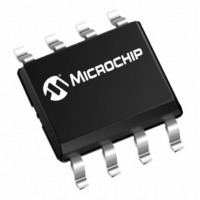
TCN75-3.3MUA Microchip Technology, TCN75-3.3MUA Datasheet - Page 16

TCN75-3.3MUA
Manufacturer Part Number
TCN75-3.3MUA
Description
IC TEMP SENSOR SRL 3.3V 8MSOP
Manufacturer
Microchip Technology
Datasheets
1.TCN75-5.0MUA.pdf
(20 pages)
2.TCN75-5.0MOA.pdf
(18 pages)
3.TCN75-5.0MUA.pdf
(30 pages)
4.TCN75AVOA.pdf
(30 pages)
Specifications of TCN75-3.3MUA
Package / Case
8-MSOP, Micro8™, 8-uMAX, 8-uSOP,
Output Type
2-Wire Serial
Function
Temp Monitoring System (Sensor)
Topology
ADC (Sigma Delta), Register Bank
Sensor Type
Internal
Sensing Temperature
-55°C ~ 125°C
Output Alarm
Yes
Output Fan
No
Voltage - Supply
2.7 V ~ 5.5 V
Operating Temperature
-55°C ~ 125°C
Mounting Type
Surface Mount
Temperature Threshold
Programmable
Full Temp Accuracy
3 C
Digital Output - Bus Interface
2-Wire
Digital Output - Number Of Bits
9 bit
Supply Voltage (max)
5.5 V
Supply Voltage (min)
2.7 V
Description/function
2-Wire Serial Input/Output - Thermal Monitors
Maximum Operating Temperature
+ 125 C
Minimum Operating Temperature
- 55 C
Supply Current
1 mA
Ic Output Type
Logic
Sensing Accuracy Range
± 0.5°C
Supply Voltage Range
2.7V To 5.5V
Sensor Case Style
MSOP
No. Of Pins
8
Filter Terminals
SMD
Rohs Compliant
Yes
Accuracy %
0.5°C
Lead Free Status / RoHS Status
Lead free / RoHS Compliant
Lead Free Status / RoHS Status
Lead free / RoHS Compliant, Lead free / RoHS Compliant
Other names
158-1003
158-1003
158-1003
Available stocks
Company
Part Number
Manufacturer
Quantity
Price
Part Number:
TCN75-3.3MUA
Manufacturer:
MICROCHIP/微芯
Quantity:
20 000
TCN75A
5.0
5.1
The TCN75A serial clock input (SCLK) and the bidirec-
tional Serial Data (SDA) line form a 2-wire bidirectional
serial port for communication.
The following bus protocol has been defined:
TABLE 5-1:
5.1.1
Data transfers are initiated by a START condition,
followed by a 7-bit device address and a 1-bit read/
write. Acknowledge (ACK) from slave confirms the
reception of each byte. Each access must be
terminated by a STOP condition.
Data transfer may be initiated when the bus is in idle.
5.1.2
The bus is controlled by a master device (typically a
microcontroller) that controls the bus access and gener-
ates the START and STOP conditions. The TCN75A is
a slave device and does not control other devices in the
bus. Both master and slave devices can operate as
either transmitter or receiver. However, the master
device determines which mode is activated.
DS21935A-page 16
Transmitter Device sending data to the bus
Receiver
Master
Slave
START
STOP
Read/Write A read or write to the TCN75A registers
ACK
NAK
Busy
Not Busy
Data Valid
Term
SERIAL COMMUNICATION
2-Wire I
DATA TRANSFER
MASTER/SLAVE
Device receiving data from the bus
The device that controls the serial bus,
typically a microcontroller
The device addressed by the master,
such as the TCN75A
A unique signal from master to initiate
serial interface with a slave
A unique signal from the master to
terminate serial interface from a slave
A receiver Acknowledges (ACK) the
reception of each byte by polling the
bus
A receiver Not-Acknowledges (NAK) or
releases the bus to show End-of-Data
(EOD)
Communication is not possible
because the bus is in use
The bus is in the idle state, both SDA
and SCLK remain high
SDA must remain stable before SCLK
becomes high in order for a data bit to
be considered valid. During normal
data transfers, SDA only changes state
while SCLK is low.
SERIAL BUS CONVENTIONS
2
C™ Compatible Interface
Description
5.1.3
A high-to-low transition of the SDA line (while SCLK is
high) is the START condition. All data transfers must be
preceded by a START condition from the master. If a
START condition is generated during data transfer, the
TCN75A resets and accepts the new START condition.
A low-to-high transition of the SDA line (while SCLK is
high) is the STOP condition. All data transfers must be
ended by a STOP condition from the master. If a STOP
condition is introduced during data transmission, the
TCN75A releases the bus.
5.1.4
Following the START condition, the host must transmit
the address byte to the TCN75A. The address for the
TCN75A is <1001,A2,A1,A0> in binary, where the
A0, A1 and A2 bits are set externally by connecting the
corresponding pins to V
address transmitted in the serial bit stream must match
the selected address for the TCN75A to respond with an
ACK.
Bit 8 in the address byte is a read/write bit. Setting this
bit to ‘1’ commands a read operation, while ‘0’
commands a write operation.
FIGURE 5-1:
5.1.5
After the start condition, each bit of data in transmission
needs to be settled for time specified by t
before SCLK toggles from low-to-high (refer to the
Serial Interface Timing Specification).
5.1.6
Each receiving device, when addressed, is obliged to
generate an acknowledge bit after the reception of
each byte. The master device must generate an extra
clock pulse for ACK to be recognized.
The acknowledging device has to pull down the SDA
line for t
SCLK from the Master and remains pulled down for
t
During read, the master must signal an End-of-Data
(EOD) to the slave by not generating an ACK bit once
the last bit has been clocked out of the slave. In this
case, the slave will leave the data line released to
enable the master to generate the STOP condition.
H-DATA
SCLK
SDA
after high-to-low transition of SCLK.
SU-DATA
Start
START/STOP CONDITION
ADDRESS BYTE
DATA VALID
ACKNOWLEDGE (ACK)
1
1
before the low-to-high transition of
Address
2
Code
0
Device Addressing.
3
0
DD
© 2005 Microchip Technology Inc.
Address Byte
4
1 A2 A1 A0
<1> or GND <0>. The 7-bit
5
Address
Slave
6
TCN75A Response
7
R/W
8
A
C
K
9
SU-DATA


