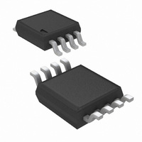
LM99-1CIMM/NOPB National Semiconductor, LM99-1CIMM/NOPB Datasheet - Page 5

LM99-1CIMM/NOPB
Manufacturer Part Number
LM99-1CIMM/NOPB
Description
IC REM DIODE TEMP SENSOR 8-MSOP
Manufacturer
National Semiconductor
Datasheet
1.LM99CIMMXNOPB.pdf
(20 pages)
Specifications of LM99-1CIMM/NOPB
Function
Hardware Monitor
Topology
ADC (Sigma Delta), Comparator, Register Bank
Sensor Type
External & Internal
Sensing Temperature
0°C ~ 125°C, External Sensor
Output Type
SMBus™
Output Alarm
Yes
Output Fan
Yes
Voltage - Supply
3 V ~ 3.6 V
Operating Temperature
0°C ~ 125°C
Mounting Type
Surface Mount
Package / Case
8-MSOP, Micro8™, 8-uMAX, 8-uSOP,
For Use With
LM99-1EVAL/NOPB - BOARD EVALUATION LM99-1LM99-1EVAL - BOARD EVALUATION LM99-1
Lead Free Status / RoHS Status
Lead free / RoHS Compliant
Other names
LM99-1CIMM
LM99-1CIMMNOPB
LM99-1CIMMNOPBTR
LM99-1CIMMNOPBTR
LM99-1CIMMTR
LM99-1CIMMNOPB
LM99-1CIMMNOPBTR
LM99-1CIMMNOPBTR
LM99-1CIMMTR
Available stocks
Company
Part Number
Manufacturer
Quantity
Price
Company:
Part Number:
LM99-1CIMM/NOPB
Manufacturer:
NS
Quantity:
978
f
t
t
t
t
t
t
t
t
t
t
t
t
SMBData, SMBCLK INPUTS
V
V
I
I
C
ALL DIGITAL OUTPUTS
I
V
SMB
LOW
HIGH
R,SMB
F,SMB
OF
TIMEOUT
SU;DAT
HD;DAT
HD;STA
SU;STO
SU;STA
BUF
IN(1)
IN(0)
OH
Symbol
Logic Electrical Characteristics
DIGITAL DC CHARACTERISTICS Unless otherwise noted, these specifications apply for V
limits apply for T
SMBus Digital Switching Characteristics
Unless otherwise noted, these specifications apply for V
pF. Boldface limits apply for T
ing characteristics of the LM99 fully meet or exceed the published specifications of the SMBus version 2.0. The following pa-
rameters are the timing relationships between SMBCLK and SMBData signals related to the LM99. They adhere to but are not
necessarily the SMBus bus specifications.
IN(1)
IN(0)
IN
OL
V
Symbol
IN(HYST)
SMBus Clock Frequency
SMBus Clock Low Time
SMBus Clock High Time
SMBus Rise Time
SMBus Fall Time
Output Fall Time
SMBData and SMBCLK Time Low for
Reset of Serial Interface (Note 14)
Data In Setup Time to SMBCLK High
Data Out Stable after SMBCLK Low
Start Condition SMBData Low to SMBCLK
Low (Start condition hold before the first
clock falling edge)
Stop Condition SMBCLK High to SMBData
Low (Stop Condition Setup)
SMBus Repeated Start-Condition Setup
Time, SMBCLK High to SMBData Low
SMBus Free Time Between Stop and Start
Conditions
Logical “1” Input Voltage
Logical “0”Input Voltage
SMBData and SMBCLK Digital
Input Hysteresis
Logical “1” Input Current
Logical “0” Input Current
Input Capacitance
High Level Output Current
SMBus Low Level Output Voltage
A
= T
J
= T
Parameter
Parameter
MIN
A
to T
= T
MAX
J
= T
; all other limits T
MIN
to T
MAX
V
V
V
I
I
OL
OL
IN
IN
OH
Conditions
; all other limits T
= 4 mA
= 6 mA
= V
= 0 V
DD
= V
from V
V
from V
(Note 12)
(Note 13)
C
I
O
IN(0)
L
A
DD
= +3.0 Vdc to +3.6 Vdc, C
= 3 mA, (Note 13)
= 400 pF,
DD
= T
max
5
IN(0)
IN(1)
J
Conditions
= +25˚C, unless otherwise noted.
max to
min to V
A
= T
IN(1)
(Note 6)
Typical
−0.005
J
0.005
min
400
= +25˚C, unless otherwise noted. The switch-
5
L
(load capacitance) on output lines = 80
(Note 6)
Typical
0.3
1
DD
= +3.0 to 3.6 Vdc. Boldface
(Note 7)
Limits
±
±
2.1
0.8
0.4
0.6
10
10
10
(Note 7)
Limits
100
250
250
300
900
100
100
4.7
4.0
0.6
1.3
10
25
25
35
www.national.com
µA (max)
µA (max)
µA (max)
V (max)
V (max)
kHz (max)
V (min)
kHz (min)
(Limit)
ms (max)
ms (max)
µs (max)
µs (max)
ns (max)
ms (min)
ns (max)
Units
µs (min)
µs (min)
ns (min)
ns (min)
ns (min)
ns (min)
µs (min)
µs (min)
(Limit)
mV
Units
pF


